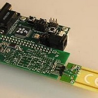
MC33696MOD434EV Freescale Semiconductor, MC33696MOD434EV Datasheet - Page 12

MC33696MOD434EV
Manufacturer Part Number
MC33696MOD434EV
Description
MCU, MPU & DSP Development Tools MC33696 (ECHO) RF C EVAL
Manufacturer
Freescale Semiconductor
Specifications of MC33696MOD434EV
Processor To Be Evaluated
MC9S08RG60
Interface Type
RS-232
Lead Free Status / RoHS Status
Lead free / RoHS Compliant
Register Access through SPI
Figure 4
slave. A received byte is considered internally on the eighth falling edge of SCLK. Consequently, the last
received bits, which do not form a complete byte, are lost.
11.3 Configuration Switching
This feature allows for defining two different configurations using two different banks, and for switching
them automatically during wakeup when using a strobe oscillator, or by means of the strobe pin actuation
by the MCU. This automatic feature may be used only in receiver mode; however, if one of the register
banks is related to a transmitter configuration, it may be accessed directly by programing some bits to
define the active bank, thus allowing fast switching between receiver mode and transmitter mode, or
between any different possible configurations.
12
(Output)
(Output)
CONFB
CONFB
(Input)
(Input)
(Input)
(Input)
SCLK
MOSI
MISO
SCLK
MOSI
MISO
SEB
SEB
and
Figure 5
A low level applied to CONFB does not affect the configuration register
contents.
N1 N0 A4 A3 A2 A1 A0 R/W
N1 N0 A4 A3 A2 A1 A0 R/W
show write and read operations in a typical SPI transfer. In both cases, the SPI is a
Figure 4. Write Operation in Configuration Mode (N[1:0] = 01)
Figure 5. Read Operation in Configuration Mode (N[1:0] = 01)
MC33696 Data Sheet, Rev. 9
D7 D6 D5 D4 D3 D2 D1
D7 D6 D5 D4 D3 D2 D1 D0
NOTE
D0
D7 D6 D5 D4 D3 D2 D1 D0
D7 D6 D5 D4 D3 D2 D1 D0
Freescale Semiconductor


