MC33696MOD434EV Freescale Semiconductor, MC33696MOD434EV Datasheet - Page 7
MC33696MOD434EV
Manufacturer Part Number
MC33696MOD434EV
Description
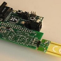
MCU, MPU & DSP Development Tools MC33696 (ECHO) RF C EVAL
Manufacturer
Freescale Semiconductor
Specifications of MC33696MOD434EV
Processor To Be Evaluated
MC9S08RG60
Interface Type
RS-232
Lead Free Status / RoHS Status
Lead free / RoHS Compliant


A second voltage regulator supplies the digital part. This regulator is powered from pin VCCDIG and its
output is connected to VCCDIG2. An external capacitor must be inserted between VCCDIG2 and
GNDDIG, for decoupling. The supply voltage VCCDIG2 is equal to 1.6 V. In standby mode, this voltage
regulator goes into an ultra-low-power mode, but VCCDIG2 = 0.7 x V
registers to be supplied, allowing configuration data to be saved.
7
At power-on, an internal reset signal is generated. All registers are reset.
When the LVDE bit is set, the low-voltage detection module is enabled. This block compares the supply
voltage on VCCINOUT with a reference level of about 1.8 V. If the voltage on VCCINOUT drops below
1.8 V, status bit LVDS is set. The information in status bit LVDS is latched and reset after a read access.
8
The receiver is based on a superheterodyne architecture with an intermediate frequency (IF) of 1.5 MHz
(see
Freescale Semiconductor
VCC2
VCC2
Figure
1
2
3
4
5
6
7
8
RSSIOUT
VCC2RF
RFIN
GNDLNA
VCC2VCO
GNDPA1
RFOUT
GNDPA2
Supply Voltage Monitoring and Reset
Receiver Functional Description
1). Its input is connected to the RFIN pin. Frequency down conversion is done by a high-side
If LVDE = 1, the LVD module remains enabled. The circuit cannot be put
in standby mode, but remains in LVD mode with a higher quiescent current,
due to the monitoring circuitry. LVD function is not accurate in standby
mode.
VCC2
3V Operation
VCC2
MC33696
U11
DATACLK
GNDDIG
CONFB
RSSIC
SCLK
MOSI
MISO
SEB
Figure 2. Wiring Diagrams
MC33696 Data Sheet, Rev. 9
24
23
22
21
20
19
18
17
3 V
NOTE
VCC2
VCC2
1
2
3
4
5
6
7
8
RSSIOUT
VCC2RF
RFIN
GNDLNA
VCC2VCO
GNDPA1
RFOUT
GNDPA2
CCDIG
Supply Voltage Monitoring and Reset
5V Operation
VCC2
VCC2
. This enables the internal
MC33696
U11
DATACLK
GNDDIG
CONFB
RSSIC
SCLK
MOSI
MISO
SEB
24
23
22
21
20
19
18
17
5 V
7
Related parts for MC33696MOD434EV
Image
Part Number
Description
Manufacturer
Datasheet
Request
R

Part Number:
Description:
Manufacturer:
Freescale Semiconductor, Inc
Datasheet:
Part Number:
Description:
Manufacturer:
Freescale Semiconductor, Inc
Datasheet:
Part Number:
Description:
Manufacturer:
Freescale Semiconductor, Inc
Datasheet:
Part Number:
Description:
Manufacturer:
Freescale Semiconductor, Inc
Datasheet:
Part Number:
Description:
Manufacturer:
Freescale Semiconductor, Inc
Datasheet:
Part Number:
Description:
Manufacturer:
Freescale Semiconductor, Inc
Datasheet:
Part Number:
Description:
Manufacturer:
Freescale Semiconductor, Inc
Datasheet:
Part Number:
Description:
Manufacturer:
Freescale Semiconductor, Inc
Datasheet:
Part Number:
Description:
Manufacturer:
Freescale Semiconductor, Inc
Datasheet:
Part Number:
Description:
Manufacturer:
Freescale Semiconductor, Inc
Datasheet:
Part Number:
Description:
Manufacturer:
Freescale Semiconductor, Inc
Datasheet:
Part Number:
Description:
Manufacturer:
Freescale Semiconductor, Inc
Datasheet:
Part Number:
Description:
Manufacturer:
Freescale Semiconductor, Inc
Datasheet:
Part Number:
Description:
Manufacturer:
Freescale Semiconductor, Inc
Datasheet:
Part Number:
Description:
Manufacturer:
Freescale Semiconductor, Inc
Datasheet: