MC33696MOD434EV Freescale Semiconductor, MC33696MOD434EV Datasheet - Page 8
MC33696MOD434EV
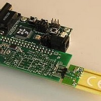
Manufacturer Part Number
MC33696MOD434EV
Description
MCU, MPU & DSP Development Tools MC33696 (ECHO) RF C EVAL
Manufacturer
Freescale Semiconductor
Specifications of MC33696MOD434EV
Processor To Be Evaluated
MC9S08RG60
Interface Type
RS-232
Lead Free Status / RoHS Status
Lead free / RoHS Compliant


Transmitter Functional Description
injection I/Q mixer driven by the frequency synthesizer. An integrated poly-phase filter performs rejection
of the image frequency.
The low intermediate frequency allows integration of the IF filter providing the selectivity. The center
frequency is tuned by automatic frequency control (AFC) referenced to the crystal oscillator frequency.
Sensitivity is met by an overall amplification of approximately 96 dB, distributed over the reception chain,
comprising low-noise amplifier (LNA), mixer, post-mixer amplifier, and IF amplifier. Automatic gain
control (AGC), on the LNA and the IF amplifier, maintains linearity and prevents internal saturation.
Sensitivity can be reduced using four programmable steps on the LNA gain.
Amplitude demodulation is achieved by peak detection and comparison with a fixed or adaptive voltage
reference selected during configuration. Frequency demodulation is achieved in two steps: the IF amplifier
AGC is disabled and acts as an amplitude limiter; a filter performs a frequency-to-voltage conversion. The
resulting signal is then amplitude demodulated in the same way as in the case of amplitude modulation
with an adaptive voltage reference.
A low-pass filter improves the signal-to-noise ratio.
Shaped data are available if the integrated data manager is not used.
If used, the data manager performs clock recovery and decoding of Manchester coded data. Data and clock
are then available on the serial peripheral interface (SPI). The configuration sets the data rate range
managed by the data manager and the bandwidth of the low-pass filter.
An internal low-frequency oscillator can be used as a strobe oscillator to perform an automatic wakeup
sequence.
It is also possible to define two different configurations for the receiver (frequency, data rate, data manager,
modulation, etc.) that are automatically loaded during wakeup or under MCU control.
If the PLL goes out of lock, received data are ignored.
9
Transmitter Functional Description
The single-ended power amplifier is connected to the RFOUT pin.
In the case of amplitude modulation, coded data sent by the microcontroller unit (MCU) are used for on/off
keying (OOK) the RF carrier. Rise and fall times of the RF signal are controlled to minimize spurious
emission.
In the case of frequency modulation, coded data sent by the MCU are used for frequency shift keying
(FSK) the RF carrier. RF output power can be reduced using four programmable steps.
Out-of-lock detection prevents any out-of-band emission, by stopping the transmission.
The logic output SWITCH enables control of an external RF switch for isolating the two RF pins. Its output
toggles when the circuit changes from receive to transmit, and vice versa.
MC33696 Data Sheet, Rev. 9
8
Freescale Semiconductor
Related parts for MC33696MOD434EV
Image
Part Number
Description
Manufacturer
Datasheet
Request
R

Part Number:
Description:
Manufacturer:
Freescale Semiconductor, Inc
Datasheet:
Part Number:
Description:
Manufacturer:
Freescale Semiconductor, Inc
Datasheet:
Part Number:
Description:
Manufacturer:
Freescale Semiconductor, Inc
Datasheet:
Part Number:
Description:
Manufacturer:
Freescale Semiconductor, Inc
Datasheet:
Part Number:
Description:
Manufacturer:
Freescale Semiconductor, Inc
Datasheet:
Part Number:
Description:
Manufacturer:
Freescale Semiconductor, Inc
Datasheet:
Part Number:
Description:
Manufacturer:
Freescale Semiconductor, Inc
Datasheet:
Part Number:
Description:
Manufacturer:
Freescale Semiconductor, Inc
Datasheet:
Part Number:
Description:
Manufacturer:
Freescale Semiconductor, Inc
Datasheet:
Part Number:
Description:
Manufacturer:
Freescale Semiconductor, Inc
Datasheet:
Part Number:
Description:
Manufacturer:
Freescale Semiconductor, Inc
Datasheet:
Part Number:
Description:
Manufacturer:
Freescale Semiconductor, Inc
Datasheet:
Part Number:
Description:
Manufacturer:
Freescale Semiconductor, Inc
Datasheet:
Part Number:
Description:
Manufacturer:
Freescale Semiconductor, Inc
Datasheet:
Part Number:
Description:
Manufacturer:
Freescale Semiconductor, Inc
Datasheet: