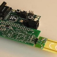
MC33696MOD434EV Freescale Semiconductor, MC33696MOD434EV Datasheet - Page 28

MC33696MOD434EV
Manufacturer Part Number
MC33696MOD434EV
Description
MCU, MPU & DSP Development Tools MC33696 (ECHO) RF C EVAL
Manufacturer
Freescale Semiconductor
Specifications of MC33696MOD434EV
Processor To Be Evaluated
MC9S08RG60
Interface Type
RS-232
Lead Free Status / RoHS Status
Lead free / RoHS Compliant
Configuration, Command, and Status Registers
17.1 Configuration Registers
Figure 19
RESET is a global reset. The bit is cleared internally, after use.
SL (Switch Level) selects the active level of the SWITCH output pin.
LVDE (Low Voltage Detection Enable) enables the low voltage detection function.
CLKE (Clock Enable) controls the DATACLK output buffer.
28
Reset Value
Bit Name
0 = no action
1 = reset all registers and counters
0 = disabled
1 = enabled
0 = DATACLK remains low
1 = DATACLK outputs F
describes configuration register 1, CONFIG1.
This bit is cleared by POR. In the event of a complete loss of the supply
voltage, LVD is disabled at power-up, but the information is not lost as the
status bit LVDS is set by POR.
LOF1
Bit 7
1
Carrier Frequency
Table 9. LOF[1:0] and CF[1:0] Setting Versus Carrier Frequency
304 MHz
315 MHz
426 MHz
434 MHz
868 MHz
915 MHz
LOF0
Bit 6
0
SL
Table 10. Active Level of SWITCH Output Pin
0
1
dataclk
Transceiver Function
Bit 5
CF1
Figure 19. CONFIG1 Register
0
MC33696 Data Sheet, Rev. 9
Transmitting
Transmitting
Receiving
Receiving
LOF1
0
1
0
0
0
1
Bit 4
CF0
NOTE
1
RESET
LOF0
Bit 3
0
0
1
1
1
1
0
Level on SWITCH
High
High
Low
Low
Bit 2
CF1
SL
0
0
0
0
0
1
1
LVDE
Bit 1
0
CF0
0
0
1
1
1
1
Freescale Semiconductor
CLKE
Bit 0
1
Addr
$00


