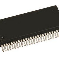
MM908E625ACDWB Freescale Semiconductor, MM908E625ACDWB Datasheet - Page 15

MM908E625ACDWB
Manufacturer Part Number
MM908E625ACDWB
Description
IC QUAD HALF BRDG MCU/LIN 54SOIC
Manufacturer
Freescale Semiconductor
Datasheets
1.MM908E625.pdf
(48 pages)
2.MM908E625ACDWB.pdf
(48 pages)
3.MM908E625ACDWB.pdf
(48 pages)
4.MM908E625ACDWB.pdf
(48 pages)
5.MM908E625ACDWB.pdf
(40 pages)
Specifications of MM908E625ACDWB
Applications
Automotive Mirror Control
Core Processor
HC08
Program Memory Type
FLASH (16 kB)
Controller Series
908E
Ram Size
512 x 8
Interface
SCI, SPI
Number Of I /o
13
Voltage - Supply
8 V ~ 18 V
Operating Temperature
-40°C ~ 85°C
Mounting Type
Surface Mount
Package / Case
54-SOIC (0.300", 7.50mm Width) Exposed Pad
Program Memory Size
16 KB
Number Of Programmable I/os
54
Number Of Timers
16
Operating Supply Voltage
- 18 V to + 28 V
Maximum Operating Temperature
+ 85 C
Mounting Style
SMD/SMT
Minimum Operating Temperature
- 40 C
Lead Free Status / RoHS Status
Contains lead / RoHS non-compliant
Available stocks
Company
Part Number
Manufacturer
Quantity
Price
Company:
Part Number:
MM908E625ACDWB
Manufacturer:
FREESCALE Semiconductor
Quantity:
26
highly integrated and cost-effective solution for automotive
and industrial applications. For automotive body electronics,
the 908E625 is well suited to perform complete mirror, door
lock, and light-levelling control all via a three-wire LIN bus.
(68HC908EY16) with flash memory together with a
SMARTMOS
combines power and control in one chip. Power switches are
provided on the SMARTMOS
terminals referred to in the following paragraphs. Also, see
the terminal diagram on
terminal locations on the package.
PORT A I/O TERMINALS (PTA0:4)
terminals that are shared with other functional modules in the
MCU. PTA0:PTA4 are shared with the keyboard interrupt
terminals, KBD0:KBD4.
and is internally connected to the SPI clock terminal of the
analog die. The PTA6/
PORT B I/O TERMINALS (PTB1, PTB3:7)
terminals that are shared with other functional modules in the
MCU. All terminals are shared with the ADC module. The
PTB6:PTB7 terminals are also shared with the Timer B
module.
of the analog die, allowing diagnostic measurements to be
calculated; e.g., current recopy, V
terminal is not accessible in this device.
PORT C I/O TERMINALS (PTC2:4)
terminals that are shared with other functional modules in the
MCU. For example, PTC2:PTC4 are shared with the ICG
module.
device and are internally connected to the MISO and MOSI
SPI terminals of the analog die.
Analog Integrated Circuit Device Data
Freescale Semiconductor
The 908E625 device was designed and developed as a
This device combines an standard HC08 MCU core
See
These terminals are special-function, bidirectional I/O port
The PTA5/SPSCK terminal is not accessible in this device
For details refer to the 68HC908EY16 datasheet.
These terminals are special-function, bidirectional I/O port
PTB0/AD0 is internally connected to the ADOUT terminal
For details refer to the 68HC908EY16 datasheet.
These terminals are special-function, bidirectional I/O port
PTC0/MISO and PTC1/MOSI are not accessible in this
For details refer to the 68HC908EY16 datasheet.
Figure 1
™
IC chip. The SMARTMOS
for a graphic representation of the various
SS
Figure 3
terminal is likewise not accessible.
™
IC configured as half-bridge
for a depiction of the
SUP
, etc. The PTB2/AD2
FUNCTIONAL TERMINAL DESCRIPTION
™
FUNCTIONAL DESCRIPTION
IC chip
INTRODUCTION
outputs with one high-side switch. Other ports are also
provided; they include Hall-effect sensor input ports, analog
input ports, and a selectable HVDD terminal. An internal
voltage regulator is provided on the SMARTMOS
which provides power to the MCU chip.
communicates using a single wire. This enables the device to
be compatible with three-wire bus systems, where one wire is
used for communication, one for battery, and the third for
ground.
PORT D I/O TERMINALS (PTD0:1)
function, bidirectional I/O port terminals that can also be
programmed to be timer terminals.
connected to the BEMF output of the analog die in order to
evaluate the BEMF signal with a special BEMF module of the
MCU.
terminal for generating the FGEN signal (PWM signal) if
required by the application.
PORT E I/O TERMINAL (PTE1)
bidirectional I/O port terminals that can also be programmed
to be enhanced serial communication.
the analog die. The connection for the receiver must be done
externally.
EXTERNAL INTERRUPT TERMINAL (IRQ)
terminal. This terminal contains an internal pull-up resistor
that is always activated, even when the
LOW.
EXTERNAL RESET TERMINAL (RST)
startup state.
entire system. It is driven LOW when any internal reset
source is asserted.
always activated, even when the reset terminal is pulled
LOW.
Also included in this device is a LIN physical layer, which
PTD1/TACH1 and PTD0/TACH0/BEMF are special-
In step motor applications the PTD0 terminal should be
PTD1 terminal is recommended for use as an output
PTE1/RXD and PTE0/TXD are special-function,
PTE0/TXD is internally connected to the TXD terminal of
The
For details refer to the 68HC908EY16 datasheet.
A Logic [0] on the
This terminal contains an internal pull-up resistor that is
For details refer to the 68HC908EY16 datasheet.
IRQ
terminal is an asynchronous external interrupt
RST
is bidirectional, allowing a reset of the
RST
terminal forces the MCU to a known
FUNCTIONAL DESCRIPTION
IRQ
terminal is pulled
INTRODUCTION
™
IC chip,
908E625
15


