MM908E625ACDWB Freescale Semiconductor, MM908E625ACDWB Datasheet - Page 16
MM908E625ACDWB
Manufacturer Part Number
MM908E625ACDWB
Description
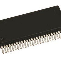
IC QUAD HALF BRDG MCU/LIN 54SOIC
Manufacturer
Freescale Semiconductor
Datasheets
1.MM908E625.pdf
(48 pages)
2.MM908E625ACDWB.pdf
(48 pages)
3.MM908E625ACDWB.pdf
(48 pages)
4.MM908E625ACDWB.pdf
(48 pages)
5.MM908E625ACDWB.pdf
(40 pages)
Specifications of MM908E625ACDWB
Applications
Automotive Mirror Control
Core Processor
HC08
Program Memory Type
FLASH (16 kB)
Controller Series
908E
Ram Size
512 x 8
Interface
SCI, SPI
Number Of I /o
13
Voltage - Supply
8 V ~ 18 V
Operating Temperature
-40°C ~ 85°C
Mounting Type
Surface Mount
Package / Case
54-SOIC (0.300", 7.50mm Width) Exposed Pad
Program Memory Size
16 KB
Number Of Programmable I/os
54
Number Of Timers
16
Operating Supply Voltage
- 18 V to + 28 V
Maximum Operating Temperature
+ 85 C
Mounting Style
SMD/SMT
Minimum Operating Temperature
- 40 C
Lead Free Status / RoHS Status
Contains lead / RoHS non-compliant
Available stocks
Company
Part Number
Manufacturer
Quantity
Price
Company:

Part Number:
MM908E625ACDWB
Manufacturer:
FREESCALE Semiconductor
Quantity:
26


CURRENT LIMITATION FREQUENCY INPUT
TERMINAL (FGEN)
high-side inrush current limiter PWM frequency. This input is
not a real PWM input terminal; it should just supply the period
of the PWM. The duty cycle will be generate automatically.
be in the range of 0.1 kHz to 20 kHz.
BACK ELECTROMAGNETIC FORCE OUTPUT
TERMINAL (BEMF)
electromagnetic force (BEMF). This feature is mainly used in
step motor applications for detecting a stalled motor. In order
to evaluate this signal the terminal must be directly connected
to terminal PTD0/TACH0/BEMF.
RESET TERMINAL (RST_A)
It is an open drain with pull-up resistor and must be
connected to the
INTERRUPT TERMINAL (IRQ_A)
indicating errors or wake-up events. It is an open drain with
pull-up resistor and must be connected to the
the MCU.
SLAVE SELECT TERMINAL (SS)
analog chip. All other SPI connections are done internally.
must be connected to PTB1 or any other logic I/O of the
microcontroller.
LIN BUS TERMINAL (LIN)
transmitter and receiver. It is suited for automotive bus
systems and is based on the LIN bus specification.
HALF-BRIDGE OUTPUT TERMINALS (HB1:HB4)
configured as four half-bridge driver outputs. The HB1:HB4
outputs may be configured for step motor drivers, DC motor
drivers, or as high-side and low-side switches.
overtemperature protected, and they feature current recopy,
current limitation, and BEMF generation. Current limitation
and recopy are done on the low-side MOSFETs.
POWER SUPPLY TERMINALS (VSUP1:VSUP3)
nominal input voltage is designed for operation from 12 V
systems. Owing to the low ON-resistance and current
16
908E625
FUNCTIONAL DESCRIPTION
FUNCTIONAL TERMINAL DESCRIPTION
Input terminal for the half-bridge current limitation and the
Important The recommended FGEN frequency should
This terminal gives the user information about back
RST_A
IRQ_A
This terminal is the SPI Slave Select terminal for the
The LIN terminal represents the single-wire bus
The 908E625 device includes power MOSFETs
The HB1:HB4 outputs are short-circuit and
VSUP1:VSUP3 are device power supply terminals. The
is the interrupt output terminal of the analog die
is the bidirectional reset terminal of the analog die.
RST
terminal of the MCU.
IRQ
terminal of
SS
requirements of the half-bridge driver outputs and high-side
output driver, multiple VSUP terminals are provided.
functionality.
POWER GROUND TERMINALS (GND1 AND GND2)
Owing to the low ON-resistance and current requirements of
the half-bridge driver outputs and high-side output driver,
multiple terminals are provided.
chip functionality.
HIGH-SIDE OUTPUT TERMINAL (HS)
The switch is protected against overtemperature and
overcurrent. The output is capable of limiting the inrush
current with an automatic PWM generation using the FGEN
module.
SWITCHABLE VDD OUTPUT TERMINAL (HVDD)
resistive loads requiring a regulated 5.0 V supply; e.g.,
3-terminal Hall-effect sensors. The output is short-circuit
protected.
HALL-EFFECT SENSOR INPUT TERMINALS
(H1:H3)
inputs for Hall-effect sensors and switches.
+5.0 V VOLTAGE REGULATOR OUTPUT
TERMINAL (VDD)
to stabilize the regulated output voltage. The VDD terminal is
intended to supply the embedded microcontroller.
supply other loads; use the HVDD terminal for this purpose.
The VDD, EVDD, VDDA, and VREFH terminals must be
connected together.
ANALOG INPUT TERMINAL (PA1)
source values.
VOLTAGE REGULATOR GROUND TERMINAL
(VSS)
of all non-power ground connections (microcontroller and
sensors).
must be connected together.
All VSUP terminals must be connected to get full chip
GND1 and GND2 are device power ground connections.
GND1 and GND2 terminals must be connected to get full
The HS output terminal is a low R
The HVDD terminal is a switchable V
The Hall-effect sensor input terminals H1:H3 provide
The VDD terminal is needed to place an external capacitor
Important The VDD terminal should not be used to
This terminal is an analog input port with selectable current
The VSS terminal is the ground terminal for the connection
Important VSS, EVSS, VSSA, and VREFL terminals
Analog Integrated Circuit Device Data
Freescale Semiconductor
DS(ON)
DD
high-side switch.
output for driving
Related parts for MM908E625ACDWB
Image
Part Number
Description
Manufacturer
Datasheet
Request
R

Part Number:
Description:
Integrated Quad Half H-bridge With Power Supply, Embedded Mcu, And Lin Serial Communication
Manufacturer:
Freescale Semiconductor, Inc
Datasheet:

Part Number:
Description:
KIT EVAL PRELIM MM98E625/26
Manufacturer:
Freescale Semiconductor
Datasheet:
Part Number:
Description:
Manufacturer:
Freescale Semiconductor, Inc
Datasheet:
Part Number:
Description:
Manufacturer:
Freescale Semiconductor, Inc
Datasheet:
Part Number:
Description:
Manufacturer:
Freescale Semiconductor, Inc
Datasheet:
Part Number:
Description:
Manufacturer:
Freescale Semiconductor, Inc
Datasheet:
Part Number:
Description:
Manufacturer:
Freescale Semiconductor, Inc
Datasheet:
Part Number:
Description:
Manufacturer:
Freescale Semiconductor, Inc
Datasheet:
Part Number:
Description:
Manufacturer:
Freescale Semiconductor, Inc
Datasheet:
Part Number:
Description:
Manufacturer:
Freescale Semiconductor, Inc
Datasheet:
Part Number:
Description:
Manufacturer:
Freescale Semiconductor, Inc
Datasheet:
Part Number:
Description:
Manufacturer:
Freescale Semiconductor, Inc
Datasheet:
Part Number:
Description:
Manufacturer:
Freescale Semiconductor, Inc
Datasheet:
Part Number:
Description:
Manufacturer:
Freescale Semiconductor, Inc
Datasheet:
Part Number:
Description:
Manufacturer:
Freescale Semiconductor, Inc
Datasheet: