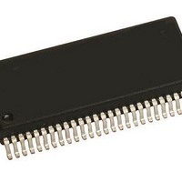
MM908E625ACDWB Freescale Semiconductor, MM908E625ACDWB Datasheet - Page 17

MM908E625ACDWB
Manufacturer Part Number
MM908E625ACDWB
Description
IC QUAD HALF BRDG MCU/LIN 54SOIC
Manufacturer
Freescale Semiconductor
Datasheets
1.MM908E625.pdf
(48 pages)
2.MM908E625ACDWB.pdf
(48 pages)
3.MM908E625ACDWB.pdf
(48 pages)
4.MM908E625ACDWB.pdf
(48 pages)
5.MM908E625ACDWB.pdf
(40 pages)
Specifications of MM908E625ACDWB
Applications
Automotive Mirror Control
Core Processor
HC08
Program Memory Type
FLASH (16 kB)
Controller Series
908E
Ram Size
512 x 8
Interface
SCI, SPI
Number Of I /o
13
Voltage - Supply
8 V ~ 18 V
Operating Temperature
-40°C ~ 85°C
Mounting Type
Surface Mount
Package / Case
54-SOIC (0.300", 7.50mm Width) Exposed Pad
Program Memory Size
16 KB
Number Of Programmable I/os
54
Number Of Timers
16
Operating Supply Voltage
- 18 V to + 28 V
Maximum Operating Temperature
+ 85 C
Mounting Style
SMD/SMT
Minimum Operating Temperature
- 40 C
Lead Free Status / RoHS Status
Contains lead / RoHS non-compliant
Available stocks
Company
Part Number
Manufacturer
Quantity
Price
Company:
Part Number:
MM908E625ACDWB
Manufacturer:
FREESCALE Semiconductor
Quantity:
26
LIN TRANSCEIVER OUTPUT TERMINAL (RXD)
must be connected to the microcontroller’s Enhanced Serial
Communications Interface (ESCI) module (RXD terminal).
ADC REFERENCE TERMINALS
(VREFL AND VREFH)
the ADC. It is recommended that a high-quality ceramic
decoupling capacitor be placed between these terminals.
ADC and should be tied to the same potential as VDDA via
separate traces. VREFL is the low reference supply for the
ADC and should be tied to the same potential as VSS via
separate traces.
ADC SUPPLY TERMINALS (VDDA AND VSSA)
analog-to-digital converter (ADC). It is recommended that a
high-quality ceramic decoupling capacitor be placed between
these terminals.
tied to the same potential as EVDD via separate traces.
Analog Integrated Circuit Device Data
Freescale Semiconductor
This terminal is the output of LIN transceiver. The terminal
VREFL and VREFH are the reference voltage terminals for
Important VREFH is the high reference supply for the
For details refer to the 68HC908EY16 datasheet.
VDDA and VSSA are the power supply terminals for the
Important VDDA is the supply for the ADC and should be
VSSA is the ground terminal for the ADC and should be tied
to the same potential as EVSS via separate traces.
MCU POWER SUPPLY TERMINALS
(EVDD AND EVSS)
terminals. The MCU operates from a single power supply.
duration current demands on the power supply. To prevent
noise problems, take special care to provide power supply
bypassing at the MCU.
TEST TERMINAL (FLSVPP)
be either left open (not connected) or connected to GND.
EXPOSED PAD TERMINAL
package conducts heat from the chip to the PCB board. For
thermal performance the pad must be soldered to the PCB
board. It is recommended that the pad be connected to the
ground potential.
For details refer to the 68HC908EY16 datasheet.
EVDD and EVSS are the power supply and ground
Fast signal transitions on MCU terminals place high, short-
For details refer to the 68HC908EY16 datasheet.
This terminal is for test purposes only. This terminal should
The exposed pad terminal on the bottom side of the
FUNCTIONAL TERMINAL DESCRIPTION
FUNCTIONAL DESCRIPTION
908E625
17


