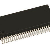
MM908E625ACDWB Freescale Semiconductor, MM908E625ACDWB Datasheet - Page 26

MM908E625ACDWB
Manufacturer Part Number
MM908E625ACDWB
Description
IC QUAD HALF BRDG MCU/LIN 54SOIC
Manufacturer
Freescale Semiconductor
Datasheets
1.MM908E625.pdf
(48 pages)
2.MM908E625ACDWB.pdf
(48 pages)
3.MM908E625ACDWB.pdf
(48 pages)
4.MM908E625ACDWB.pdf
(48 pages)
5.MM908E625ACDWB.pdf
(40 pages)
Specifications of MM908E625ACDWB
Applications
Automotive Mirror Control
Core Processor
HC08
Program Memory Type
FLASH (16 kB)
Controller Series
908E
Ram Size
512 x 8
Interface
SCI, SPI
Number Of I /o
13
Voltage - Supply
8 V ~ 18 V
Operating Temperature
-40°C ~ 85°C
Mounting Type
Surface Mount
Package / Case
54-SOIC (0.300", 7.50mm Width) Exposed Pad
Program Memory Size
16 KB
Number Of Programmable I/os
54
Number Of Timers
16
Operating Supply Voltage
- 18 V to + 28 V
Maximum Operating Temperature
+ 85 C
Mounting Style
SMD/SMT
Minimum Operating Temperature
- 40 C
Lead Free Status / RoHS Status
Contains lead / RoHS non-compliant
Available stocks
Company
Part Number
Manufacturer
Quantity
Price
Company:
Part Number:
MM908E625ACDWB
Manufacturer:
FREESCALE Semiconductor
Quantity:
26
ANALOG DIE I/OS
LIN Physical Layer
wire communication in automotive applications. The LIN
physical layer is designed to meet the LIN physical layer
specification.
limitation and thermal shutdown. An internal pull-up resistor
with a serial diode structure is integrated, so no external pull-
up components are required for the application in a slave
node. The fall time from dominant to recessive and the rise
time from recessive to dominant is controlled. The symmetry
between both slew rate controls is guaranteed.
from external disturbance, guaranteeing communication
during external disturbance.
PSON bit in the System Control Register (SYSCTL). If the
transmitter works in the current limitation region, the LINCL
bit in the System Status Register (SYSSTAT) is set. Due to
excessive power dissipation in the transmitter, software is
advised to monitor this bit and turn the transmitter off
immediately.
TXD TERMINAL
of the LIN transmitter (see
output is low (dominant state). When TXD is HIGH, the LIN
output MOSFET is turned off. The TXD terminal has an
internal pull-up current source in order to set the LIN bus in
recessive state in the event, for instance, the microcontroller
could not control it during system power-up or power-down.
RXD TERMINAL
reports the state of the LIN bus voltage. LIN HIGH (recessive
state) is reported by a high level on RXD, LIN LOW (dominant
state) by a low level on RXD.
STOP MODE/WAKE-UP FEATURE
physical layer is disabled. The receiver terminal is still active
and able to detect wake-up events on the LIN bus line.
Register is set), a falling edge on the LIN line causes an
interrupt. This interrupt switches on the main voltage
regulator and generates a system wake-up.
26
908E625
FUNCTIONAL DEVICE OPERATION
LOGIC COMMANDS AND REGISTERS
The LIN bus terminal provides a physical layer for single-
The LIN driver is a low-side MOSFET with internal current
The LIN terminal offers high susceptibility immunity level
The LIN transmitter circuitry is enabled by setting the
The TXD terminal is the MCU interface to control the state
The RXD transceiver terminal is the MCU interface, which
During STOP mode operation the transmitter of the
If LIN interrupt is enabled (LINIE bit in the Interrupt Mask
Figure
1). When TXD is LOW, LIN
Analog Multiplexer/ADOUT Terminal
ADC of the MCU. See
used to read seven internal diagnostic analog voltages.
Current Recopy
current sense circuits of the half-bridges. These sense
circuits offer a voltage proportional to the current through the
low-side MOSFET. High or low resolution is selectable:
5.0 V/2.5 A or 5.0 V/500 mA, respectively. Refer to
Bridge Current
Analog Input PA1
multiplexer, permitting analog values from the periphery to be
read.
TEMPERATURE SENSOR
This sensor offers a voltage that is proportional to the actual
chip junction temperature.
V
of the external supply voltage. The output of this voltage is
V
selected with the ADMUX Register.
ANALOG MULTIPLEXER CONFIGURATION
REGISTER (ADMUX)
SS3, SS2, SS1, and SS0—A/D Input Select Bits
microcontroller according to
SS1, and SS0 bits.
Reset
Read
Write
SUP
SUP
Bits
The ADOUT terminal is the analog output interface to the
The analog multiplexer is connected to the four low-side
The analog input PA1 is directly connected to the analog
The 908E625 includes an on-chip temperature sensor.
The V
The different internal diagnostic analog voltages can be
These read/write bits select the input to the ADC in the
/RATIO
PRESCALER
SUP
7
0
0
Register Name and Address: ADMUX - $07
VSUP
prescaler permits the reading or measurement
Recopy.)
6
0
0
.
Analog Integrated Circuit Device Data
Figure
5
0
0
Table
12. An analog multiplexer is
4
0
0
7. Reset clears SS3, SS2,
Freescale Semiconductor
SS3
3
0
SS2
2
0
SS1
1
0
Half-
SS0
0
0


