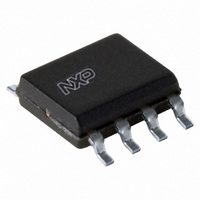
PHC2300,118 NXP Semiconductors, PHC2300,118 Datasheet - Page 3

PHC2300,118
Manufacturer Part Number
PHC2300,118
Description
MOSFET N/P-CH 300V 340MA SOT96-1
Manufacturer
NXP Semiconductors
Datasheet
1.PHC2300118.pdf
(14 pages)
Specifications of PHC2300,118
Fet Type
N and P-Channel
Fet Feature
Logic Level Gate
Rds On (max) @ Id, Vgs
6 Ohm @ 170mA, 10V
Drain To Source Voltage (vdss)
300V
Current - Continuous Drain (id) @ 25° C
340mA
Vgs(th) (max) @ Id
2V @ 1mA
Gate Charge (qg) @ Vgs
6.24nC @ 10V
Input Capacitance (ciss) @ Vds
102pF @ 50V
Power - Max
1.6W
Mounting Type
Surface Mount
Package / Case
8-SOIC (3.9mm Width)
Lead Free Status / RoHS Status
Lead free / RoHS Compliant
Other names
934054090118
PHC2300 /T3
PHC2300 /T3
PHC2300 /T3
PHC2300 /T3
NXP Semiconductors
4. Limiting values
Table 4.
In accordance with the Absolute Maximum Rating System (IEC 60134).
[1]
[2]
[3]
[4]
[5]
[6]
PHC2300
Product data sheet
Symbol
V
V
I
I
P
T
T
D
DM
Fig 1.
stg
j
DS
GS
tot
Solder point temperature is the temperature at the soldering point of the drain leads.
Pulse width and duty cycle limited by maximum junction temperature.
Maximum permissible dissipation per MOS transistor (both devices may thus be loaded up to 1.6 W at the same time).
Maximum permissible dissipation per MOS transistor. Value based on a printed-circuit board with an R
27.5 K/W.
Maximum permissible dissipation per MOS transistor. Value based on a printed-circuit board with an R
K/W.
Maximum permissible dissipation if only one MOS transistor dissipates. Value based on a printed-circuit board with an R
to tie-point) of 90 K/W.
P
(W)
1.6
1.2
0.8
0.4
tot
2
0
Power derating curve
0
Limiting values
Parameter
drain-source voltage
gate-source voltage
drain current
peak drain current
total power dissipation
storage temperature
junction temperature
40
80
120
All information provided in this document is subject to legal disclaimers.
T
s
mda235
(°C)
Rev. 05 — 24 February 2011
160
Conditions
T
T
T
T
T
T
T
T
T
T
j
j
sp
sp
sp
sp
sp
amb
amb
amb
≥ 25 °C; T
≥ 25 °C; T
= 80 °C; N-channel
= 80 °C; P-channel
= 25 °C; pulsed; N-channel
= 25 °C; pulsed; P-channel
= 80 °C
= 25 °C
= 25 °C
= 25 °C
Complementary enhancement mode MOS transistors
j
j
Fig 2.
≤ 150 °C; N-channel
≤ 150 °C; P-channel
10 −
10 −
10 −
(A)
I
10
D
1
1
2
3
δ = 0.01; T
(1) R
SOAR; N-channel
1
P
(1)
DSon
t
p
T
limitation.
sp
10
= 80 °C.
δ =
t
T
t
p
th(a-tp)
th(a-tp)
[1]
[1]
[2]
[2]
[3]
[4]
[5]
[6]
DC
10
Min
-
-
-20
-
-
-
-
-
-
-
-
-55
-55
(ambient to tie-point) of 90
(ambient to tie-point) of
2
PHC2300
V
© NXP B.V. 2011. All rights reserved.
DS
(V)
mda240
150
150
Max
300
-300
20
340
-235
1.4
-0.9
1.6
1.8
0.9
1.2
th(a-tp)
10
3
(ambient
Unit
V
V
V
mA
mA
A
A
W
W
W
W
°C
°C
3 of 14


