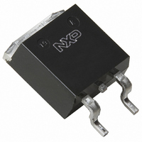
PSMN009-100B,118 NXP Semiconductors, PSMN009-100B,118 Datasheet - Page 5

PSMN009-100B,118
Manufacturer Part Number
PSMN009-100B,118
Description
MOSFET N-CH 100V 75A D2PAK
Manufacturer
NXP Semiconductors
Series
TrenchMOS™r
Datasheet
1.PSMN009-100B118.pdf
(13 pages)
Specifications of PSMN009-100B,118
Package / Case
D²Pak, TO-263 (2 leads + tab)
Mounting Type
Surface Mount
Power - Max
230W
Fet Type
MOSFET N-Channel, Metal Oxide
Gate Charge (qg) @ Vgs
156nC @ 10V
Vgs(th) (max) @ Id
4V @ 1mA
Current - Continuous Drain (id) @ 25° C
75A
Drain To Source Voltage (vdss)
100V
Fet Feature
Standard
Rds On (max) @ Id, Vgs
8.8 mOhm @ 25A, 10V
Minimum Operating Temperature
- 55 C
Configuration
Single
Transistor Polarity
N-Channel
Resistance Drain-source Rds (on)
0.0088 Ohm @ 10 V
Drain-source Breakdown Voltage
100 V
Gate-source Breakdown Voltage
20 V
Continuous Drain Current
75 A
Power Dissipation
230000 mW
Maximum Operating Temperature
+ 175 C
Mounting Style
SMD/SMT
Lead Free Status / RoHS Status
Lead free / RoHS Compliant
Lead Free Status / RoHS Status
Lead free / RoHS Compliant, Lead free / RoHS Compliant
Other names
934057045118::PSMN009-100B /T3::PSMN009-100B /T3
NXP Semiconductors
5. Thermal characteristics
Table 5.
PSMN009-100B_2
Product data sheet
Symbol
R
R
Fig 4.
th(j-mb)
th(j-a)
Transient thermal impedance from junction to mounting base as a function of pulse duration
Thermal characteristics
Parameter
thermal resistance from junction
to mounting base
thermal resistance from junction
to ambient
Z
(K/W)
th(j-mb)
10
10
10
−1
−2
−3
1
10
−6
0.02
δ = 0.5
0.2
0.1
0.05
single pulse
10
−5
10
−4
Conditions
see
minimum footprint; mounted on
a printed-circuit board
Rev. 02 — 6 July 2009
Figure 4
10
−3
N-channel TrenchMOS SiliconMAX standard level FET
10
−2
10
−1
P
t
p
1
PSMN009-100B
T
Min
-
-
t
δ =
p
(s)
03af48
T
t
t
p
10
Typ
-
50
© NXP B.V. 2009. All rights reserved.
Max
0.65
-
Unit
K/W
K/W
5 of 13


