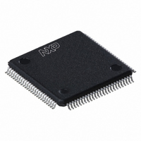
TDA9955HL/17/C1:55 NXP Semiconductors, TDA9955HL/17/C1:55 Datasheet - Page 32

TDA9955HL/17/C1:55
Manufacturer Part Number
TDA9955HL/17/C1:55
Description
TDA9955HL/LQFP100/TRAYBDP//17/
Manufacturer
NXP Semiconductors
Type
Videor
Datasheet
1.TDA9955HL17C151.pdf
(52 pages)
Specifications of TDA9955HL/17/C1:55
Resolution (bits)
8 b
Sampling Rate (per Second)
170M
Data Interface
Serial
Voltage Supply Source
Analog and Digital
Voltage - Supply
1.75 V ~ 1.85 V, 3.15 V ~ 3.45 V
Operating Temperature
0°C ~ 70°C
Mounting Type
Surface Mount
Package / Case
100-LQFP
Lead Free Status / RoHS Status
Lead free / RoHS Compliant
Other names
935281545551
TDA9955HL/17/C1-S
TDA9955HL/17/C1-S
TDA9955HL/17/C1-S
TDA9955HL/17/C1-S
Available stocks
Company
Part Number
Manufacturer
Quantity
Price
Company:
Part Number:
TDA9955HL/17/C1:55
Manufacturer:
NXP Semiconductors
Quantity:
10 000
NXP Semiconductors
Table 36.
Legend: * = default value
Table 37.
Legend: * = default value
[1]
Table 38.
Legend: * = default value
TDA9955HL_1
Product data sheet
Addr Register
CEh
CFh
D0h
Address Register
D1h
D2h
D3h
Addr Register
D4h
D5h
D6h
The minimum width of the gain pulse (GAIN_END
pulse and the clamp pulse should not overlap.
CLP_F2_LINE_S_MSB 7 to 3 -
CLP_F2_LINE_S_LSB 7 to 0 CLAMP_F2_LINE_START[7:0]
CLP_F2_LINE_WIDTH 7 to 0 CLAMP_F2_LINE_WIDTH[7:0]
FDW_S_LSB
FDW_MSB
FDW_E_LSB
GAIN_S_LSB 7 to 0 GAIN_START[7:0]
GAIN_MSB
GAIN_E_LSB 7 to 0 GAIN_END[7:0]
CLP_Fx_LINE_nnn registers (address CBh to D0h) bit description
GAIN signal registers (address D1h to D3h) bit description
Horizontal sync registers (address D4h to D6h) bit description
Bit
7 to 0 FDW_START[7:0]
7 to 4 FDW_START[11:8]
3 to 0 FDW_END[11:8]
7 to 0 FDW_END[7:0]
Bit
7 to 4 GAIN_ START[11:8] W
3 to 0 GAIN_ END[11:8]
Symbol
Bit
2 to 0 CLAMP_F2_LINE_START[10:8] W
Symbol
Symbol
Rev. 01 — 17 March 2008
GAIN_START) is 80 pixels and can include the horizontal sync pulse. The gain
Access Value Description
W
W
W
W
Access Value Description
W
W
W
Triple 8-bit analog-to-digital video converter for HDTV
00h*
0h*
0h*
00h*
00h*
0h*
0h*
51h*
frame detection window start: position of the start
of the frame detection window; the recommended
value is
frame detection window end: position of the end of
the frame detection window; the recommended value
is
3
gain start signal: position of the gain signal
generated by the timing generator
gain end signal: position of the end of the gain
signal generated by the timing generator
8
Access Value Description
W
W
W
[1]
of total number of pixels per line
7
8
of total number of pixels per line
…continued
0
0000*
000*
00h*
00h*
not used
clamp signal line start for
field 2 (LSB): position, in
number of lines, from which no
clamp pulses are generated for
field 2, typically during the
vertical pulse in case of the
sync on green signal
clamp signal line width for
field 2: width, in number of
lines, where no clamp pulses
are generated for field 2
TDA9955HL
© NXP B.V. 2008. All rights reserved.
32 of 52


