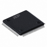
TDA9955HL/17/C1:55 NXP Semiconductors, TDA9955HL/17/C1:55 Datasheet - Page 40

TDA9955HL/17/C1:55
Manufacturer Part Number
TDA9955HL/17/C1:55
Description
TDA9955HL/LQFP100/TRAYBDP//17/
Manufacturer
NXP Semiconductors
Type
Videor
Datasheet
1.TDA9955HL17C151.pdf
(52 pages)
Specifications of TDA9955HL/17/C1:55
Resolution (bits)
8 b
Sampling Rate (per Second)
170M
Data Interface
Serial
Voltage Supply Source
Analog and Digital
Voltage - Supply
1.75 V ~ 1.85 V, 3.15 V ~ 3.45 V
Operating Temperature
0°C ~ 70°C
Mounting Type
Surface Mount
Package / Case
100-LQFP
Lead Free Status / RoHS Status
Lead free / RoHS Compliant
Other names
935281545551
TDA9955HL/17/C1-S
TDA9955HL/17/C1-S
TDA9955HL/17/C1-S
TDA9955HL/17/C1-S
Available stocks
Company
Part Number
Manufacturer
Quantity
Price
Company:
Part Number:
TDA9955HL/17/C1:55
Manufacturer:
NXP Semiconductors
Quantity:
10 000
NXP Semiconductors
TDA9955HL_1
Product data sheet
Table 52.
Legend: * = default value
Table 53.
Legend: * = default value
Table 54.
Legend: * = default value
Table 55.
Legend: * = default value
Bit
1
0
Bit
7 to 1 -
0
Bit
7 to 0 LSB_SEL
Bit
7 and 6
Symbol
PD_ADC_GY W
PD_ADC_RV W
Symbol
FVH_SEL
Symbol
Symbol Access Value Description
-
PD_AVI_CTRL1 register (address F5h) bit description
FVH_SEL register (address F6h) bit description
LSB_OUT_SEL register (address F7h) bit description
ORX_SEL register (address F9h) bit description
W
Access Value Description
Access Value Description
W
W
Rev. 01 — 17 March 2008
Access Value Description
W
00
01
10
0*
1
0*
1
-
0
1*
00h*
81h
82h
Triple 8-bit analog-to-digital video converter for HDTV
Orr signals: selects the signal applied on internal Orr (over
range channel red) signal
power-down G/Y ADC: enables the power-down of the
green channel (G/Y) ADC
power-down R/P
red channel (R/P
not used
timing signals: defiines the output on pins 15, 16 and 17
or_rv_agc: an ADC output underflow or overflow of the
range defined by the registers 22h and 23h
or_rv_datapath: an ADC output underflow or overflow of
the range defined by the registers E1h and E2h
gain: monitors the gain calibration signal. see
and
normal operation
Power-down mode
normal operation
Power-down mode
HREF; VREF; FREF
HS; VS; CS
LSB signal: selects the signal on the LSB pin of each
digital port (pins 75, 88 and 100).
Figure 13
VPA[0]; VPB[0]; VPC[0]
HREF; VREF; FREF
ORGY; ORBU; ORRV
R
R
) ADC
ADC: enables the power-down of the
[1][2]
…continued
TDA9955HL
© NXP B.V. 2008. All rights reserved.
Figure 12
40 of 52


