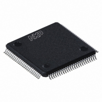
TDA9955HL/17/C1:55 NXP Semiconductors, TDA9955HL/17/C1:55 Datasheet - Page 7

TDA9955HL/17/C1:55
Manufacturer Part Number
TDA9955HL/17/C1:55
Description
TDA9955HL/LQFP100/TRAYBDP//17/
Manufacturer
NXP Semiconductors
Type
Videor
Datasheet
1.TDA9955HL17C151.pdf
(52 pages)
Specifications of TDA9955HL/17/C1:55
Resolution (bits)
8 b
Sampling Rate (per Second)
170M
Data Interface
Serial
Voltage Supply Source
Analog and Digital
Voltage - Supply
1.75 V ~ 1.85 V, 3.15 V ~ 3.45 V
Operating Temperature
0°C ~ 70°C
Mounting Type
Surface Mount
Package / Case
100-LQFP
Lead Free Status / RoHS Status
Lead free / RoHS Compliant
Other names
935281545551
TDA9955HL/17/C1-S
TDA9955HL/17/C1-S
TDA9955HL/17/C1-S
TDA9955HL/17/C1-S
Available stocks
Company
Part Number
Manufacturer
Quantity
Price
Company:
Part Number:
TDA9955HL/17/C1:55
Manufacturer:
NXP Semiconductors
Quantity:
10 000
NXP Semiconductors
8. Functional description
TDA9955HL_1
Product data sheet
8.2.1 Clamps
8.2.2 ADCs
8.2.3 Automatic Gain Control (AGC)
8.1 Analog multiplexers
8.2 R/P
8.3 Sync slicing
This high-rate front end is designed to convert analog signals coming from an analog
source (RGB or YUV) into parallel digital data used by media processor ICs such as the
NXP Semiconductors Nexperia devices for HDTV or by other video signal ICs. The
high-rate front end is able to output RGB 4 : 4 : 4, YUV 4 : 4 : 4, YUV 4 : 2 : 2 semi-planar
and YUV 4 : 2 : 2 ITU-R BT.656 formats and accepts progressive and interlaced input
formats. The high-rate front end also contains a RGB-to-YUV and YUV-to-RGB
conversion matrix, downsampling filters and range control function.
The choice between the two analog video inputs is either automatic (activity detection) or
controlled by the I
HCSYNCx and VSYNCx (where x equals 1 or 2).
Three independent parallel clamping circuits are used to clamp the video input signals on
programmable black/blanking levels. The clamp level of each channel can be changed
from 0 to 191 in steps of 1 LSB. The clamp signal comes from the VHREF timing
generator or from the CLAMP pin.
The clamping circuits can be inhibited during the vertical sync pulse and also during false
black/blanking level in the end of active video signal in a frame/field.
Three ADCs convert analog signals into three series of 8-bit codes, with a maximum
sampling frequency of 170 MHz. The ADCs input range is 1 V (p-p).
During the gain calibration pulse period, the ADCs are used to calibrate the video
amplifiers and during the clamp active period the ADCs are used to set the clamp level to
the desired values.
Gain registers, one per channel, control directly the gain of each video amplifier. The
programming of these registers is done by I
the next horizontal synchronization pulse. These contrast registers are programmable
from 0 dB to 5 dB (gain registers on 11 bits).
The gain calibration control signal comes from the VHREF timing generator.
Two sync slicers extract the composite sync from the green, luminance or CVBS signal
through SOGx pins. This synchronization signal can be bi-level or tri-level.
R
, B/P
B
and G/Y channels
2
C-bus. An analog video input is defined by pins SOGx, Rx, Bx, Gx,
Rev. 01 — 17 March 2008
Triple 8-bit analog-to-digital video converter for HDTV
2
C-bus and their content is validated only on
TDA9955HL
© NXP B.V. 2008. All rights reserved.
7 of 52


