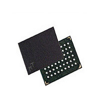
MT45W512KW16PGA-70 WT Micron Technology Inc, MT45W512KW16PGA-70 WT Datasheet - Page 11

MT45W512KW16PGA-70 WT
Manufacturer Part Number
MT45W512KW16PGA-70 WT
Description
Manufacturer
Micron Technology Inc
Datasheet
1.MT45W512KW16PGA-70_WT.pdf
(24 pages)
Specifications of MT45W512KW16PGA-70 WT
Operating Temperature (max)
85C
Mounting
Surface Mount
Operating Temperature Classification
Commercial
Lead Free Status / RoHS Status
Compliant
Configuration Register (CR) Operation
Access Using ZZ#
Figure 9:
Software Access to the Configuration Register
PDF: 09005aef8220472e/Source: 09005aef8220461e
8mb_asyncpage_ps1_0_p23z.fm - Rev. A 7/06 EN
Load Configuration Register Operation
The CR defines how the PSRAM device performs its transparent self refresh. Altering the
refresh parameters can dramatically reduce current consumption during standby mode.
Page mode control is also embedded into the CR. This register can be updated any time
the device is operating in a standby state. Figure 12 on page 13 describes the control bits
used in the CR. At power-up, the CR is set to 0010h.
The CR can be loaded using a WRITE operation immediately after ZZ# makes a HIGH-
to-LOW transition (see Figure 9). The values placed on addresses A[18:0] are latched into
the CR on the rising edge of CE# or WE#, whichever occurs first. LB#/UB# are “Don’t
Care.” Access using ZZ# is WRITE only.
ADDRESS
The contents of the CR can either be read or modified using a software sequence. The
nature of this access mechanism may eliminate the need for the ZZ# ball.
If the software mechanism is used, ZZ# can simply be tied to V
cally used for ZZ# control purposes will no longer be required. However, ZZ# should not
be tied to V
software access sequence.
The CR is loaded using a four-step sequence consisting of two READ operations followed
by two WRITE operations (see Figure 10 on page 12). The read sequence is virtually iden-
tical except that an asynchronous READ is performed during the fourth operation (see
Figure 11 on page 12). Note that a third READ cycle of the highest address will cancel the
access sequence until a different address is read.
The address used during all READ and WRITE operations is the highest address of the
PSRAM device being accessed (7FFFFh for 8Mb); the content of this address is not
changed by using this sequence. The data bus is used to transfer data into or out of bits
15–0 of the CR.
Writing to the CR using the software sequence modifies the function of the ZZ# ball.
Once the software sequence loads the CR, the level of the ZZ# ball no longer enables PAR
operation. PAR operation will be updated whenever the software sequence loads a new
value into the CR. This ZZ# functionality will continue until the next time the device is
powered up. The operation of the ZZ# ball is not affected if the software sequence is only
used to read the contents of the CR. The use of the software sequence does not affect the
ability to perform the standard (ZZ#-controlled) method of loading the CR.
WE#
CE#
ZZ#
CC
t < 500ns
Q if the system will use DPD; DPD cannot be enabled or disabled using the
ADDRESS VALID
11
Configuration Register (CR) Operation
Micron Technology, Inc., reserves the right to change products or specifications without notice.
8Mb: 512K x 16 Async/Page PSRAM
©2006 Micron Technology, Inc. All rights reserved.
CC
Q. The port line typi-
Advance


