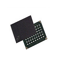
MT45W512KW16PGA-70 WT Micron Technology Inc, MT45W512KW16PGA-70 WT Datasheet - Page 3

MT45W512KW16PGA-70 WT
Manufacturer Part Number
MT45W512KW16PGA-70 WT
Description
Manufacturer
Micron Technology Inc
Datasheet
1.MT45W512KW16PGA-70_WT.pdf
(24 pages)
Specifications of MT45W512KW16PGA-70 WT
Operating Temperature (max)
85C
Mounting
Surface Mount
Operating Temperature Classification
Commercial
Lead Free Status / RoHS Status
Compliant
Ball Descriptions
Table 1:
PDF: 09005aef8220472e/Source: 09005aef8220461e
8mb_asyncpage_ps1_0_p23z.fm - Rev. A 7/06 EN
H4, H3, H2, D4,
F3, G4, G3, H5,
D2, C2, C1, B1,
H1, D3, E4, F4,
C4, C3, B4, B3,
G1, F1, F2, E2,
G6, F6, F5, E5,
D5, C6, C5, B6
Assignment
VFBGA Ball
A5, A4, A3
H6, E3, G2
A6
B5
A2
G5
A1
B2
D6
D1
E1
E6
VFBGA Ball Descriptions
DQ[15:0]
Symbol
A[18:0]
V
V
WE#
OE#
UB#
ZZ#
CE#
LB#
V
V
NC
CC
SS
CC
SS
Q
Q
Output
Supply
Supply
Supply
Supply
Input/
Input
Input
Input
Input
Input
Input
Input
Type
Address inputs: Inputs for the address accessed during READ or WRITE
operations. The address lines are also used to define the value to be loaded into
the CR.
Sleep enable: When ZZ# is LOW, the CR can be loaded or the device can enter
one of two low-power modes (DPD or PAR).
Chip enable: Activates the device when LOW. When CE# is HIGH, the device is
disabled and goes into standby power mode.
Output enable: Enables the output buffers when LOW. When OE# is HIGH, the
output buffers are disabled.
Write enable: Enables WRITE operations when LOW.
Lower byte enable: DQ[7:0]
Upper byte enable: DQ[15:8]
Data inputs/outputs.
Not internally connected.
Device power supply: (1.7V–1.95V) Power supply for device core operation.
I/O power supply: (1.7V–3.6V) Power supply for input/output buffers.
V
V
SS
SS
Q must be connected to ground.
must be connected to ground.
3
Micron Technology, Inc., reserves the right to change products or specifications without notice.
8Mb: 512K x 16 Async/Page PSRAM
Description
©2006 Micron Technology, Inc. All rights reserved.
Ball Descriptions
Advance


