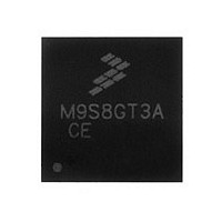
MC9S08GT32ACFDE Freescale, MC9S08GT32ACFDE Datasheet - Page 183

MC9S08GT32ACFDE
Manufacturer Part Number
MC9S08GT32ACFDE
Description
Manufacturer
Freescale
Datasheet
1.MC9S08GT32ACFDE.pdf
(302 pages)
Specifications of MC9S08GT32ACFDE
Cpu Family
HCS08
Device Core Size
8b
Frequency (max)
40MHz
Interface Type
I2C/SCI/SPI
Total Internal Ram Size
2KB
# I/os (max)
39
Number Of Timers - General Purpose
4
Operating Supply Voltage (typ)
2.5/3.3V
Operating Supply Voltage (max)
3.6V
Operating Supply Voltage (min)
1.8/2.08V
On-chip Adc
8-chx10-bit
Instruction Set Architecture
CISC
Operating Temp Range
-40C to 85C
Operating Temperature Classification
Industrial
Mounting
Surface Mount
Pin Count
48
Package Type
QFN EP
Program Memory Type
Flash
Program Memory Size
32KB
Lead Free Status / RoHS Status
Compliant
- Current page: 183 of 302
- Download datasheet (8Mb)
11.3
The SCI allows full-duplex, asynchronous, NRZ serial communication among the MCU and remote
devices, including other MCUs. The SCI comprises a baud rate generator, transmitter, and receiver block.
The transmitter and receiver operate independently, although they use the same baud rate generator.
During normal operation, the MCU monitors the status of the SCI, writes the data to be transmitted, and
processes received data. The following describes each of the blocks of the SCI.
11.3.1
As shown in
SCI communications require the transmitter and receiver (which typically derive baud rates from
independent clock sources) to use the same baud rate. Allowed tolerance on this baud frequency depends
on the details of how the receiver synchronizes to the leading edge of the start bit and how bit sampling is
performed.
The MCU resynchronizes to bit boundaries on every high-to-low transition, but in the worst case, there are
no such transitions in the full 10- or 11-bit time character frame so any mismatch in baud rate is
accumulated for the whole character time. For a Freescale Semiconductor SCI system whose bus
frequency is driven by a crystal, the allowed baud rate mismatch is about ±4.5 percent for 8-bit data format
and about ±4 percent for 9-bit data format. Although baud rate modulo divider settings do not always
produce baud rates that exactly match standard rates, it is normally possible to get within a few percent,
which is acceptable for reliable communications.
11.3.2
This section describes the overall block diagram for the SCI transmitter
specialized functions for sending break and idle characters.
The transmitter is enabled by setting the TE bit in SCIxC2. This queues a preamble character that is one
full character frame of the idle state. The transmitter then remains idle until data is available in the transmit
data buffer. Programs store data into the transmit data buffer by writing to the SCI data register (SCIxD).
The central element of the SCI transmitter is the transmit shift register that is either 10 or 11 bits long
depending on the setting in the M control bit. For the remainder of this section, we will assume M = 0,
selecting the normal 8-bit data mode. In 8-bit data mode, the shift register holds a start bit, eight data bits,
and a stop bit. When the transmit shift register is available for a new SCI character, the value waiting in
Freescale Semiconductor
Functional Description
Baud Rate Generation
Transmitter Functional Description
Figure
BUSCLK
11-12, the clock source for the SCI baud rate generator is the bus-rate clock.
BAUD RATE GENERATOR
OFF IF [SBR12:SBR0] = 0
MODULO DIVIDE BY
(1 THROUGH 8191)
Figure 11-12. SCI Baud Rate Generation
SBR12:SBR0
MC9S08GB60A Data Sheet, Rev. 2
BAUD RATE =
DIVIDE BY
16
Rx SAMPLING CLOCK
(16 × BAUD RATE)
[SBR12:SBR0] × 16
BUSCLK
Tx BAUD RATE
Serial Communications Interface (S08SCIV1)
(Figure
11-2), as well as
183
Related parts for MC9S08GT32ACFDE
Image
Part Number
Description
Manufacturer
Datasheet
Request
R

Part Number:
Description:
TOWER ELEVATOR BOARDS HARDWARE
Manufacturer:
Freescale Semiconductor
Datasheet:

Part Number:
Description:
TOWER SERIAL I/O HARDWARE
Manufacturer:
Freescale Semiconductor
Datasheet:

Part Number:
Description:
LCD MODULE FOR TWR SYSTEM
Manufacturer:
Freescale Semiconductor
Datasheet:

Part Number:
Description:
DAUGHTER LCD WVGA I.MX51
Manufacturer:
Freescale Semiconductor
Datasheet:

Part Number:
Description:
TOWER SYSTEM BOARD MPC5125
Manufacturer:
Freescale Semiconductor
Datasheet:

Part Number:
Description:
KIT EVALUATION I.MX51
Manufacturer:
Freescale Semiconductor
Datasheet:

Part Number:
Description:
KIT DEVELOPMENT WINCE IMX25
Manufacturer:
Freescale Semiconductor
Datasheet:

Part Number:
Description:
TOWER SYSTEM KIT MPC5125
Manufacturer:
Freescale Semiconductor
Datasheet:

Part Number:
Description:
TOWER SYSTEM BOARD K40X256
Manufacturer:
Freescale Semiconductor
Datasheet:

Part Number:
Description:
TOWER SYSTEM KIT K40X256
Manufacturer:
Freescale Semiconductor
Datasheet:

Part Number:
Description:
Microcontrollers (MCU) MX28 PLATFORM DEV KIT
Manufacturer:
Freescale Semiconductor
Datasheet:

Part Number:
Description:
MCU, MPU & DSP Development Tools IAR KickStart Kit for Kinetis K60
Manufacturer:
Freescale Semiconductor
Datasheet:

Part Number:
Description:
24BIT HDMI MX535/08
Manufacturer:
Freescale Semiconductor
Datasheet:
Part Number:
Description:
Manufacturer:
Freescale Semiconductor, Inc
Datasheet:
Part Number:
Description:
Manufacturer:
Freescale Semiconductor, Inc
Datasheet:


