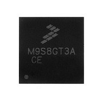
MC9S08GT32ACFDE Freescale, MC9S08GT32ACFDE Datasheet - Page 231

MC9S08GT32ACFDE
Manufacturer Part Number
MC9S08GT32ACFDE
Description
Manufacturer
Freescale
Datasheet
1.MC9S08GT32ACFDE.pdf
(302 pages)
Specifications of MC9S08GT32ACFDE
Cpu Family
HCS08
Device Core Size
8b
Frequency (max)
40MHz
Interface Type
I2C/SCI/SPI
Total Internal Ram Size
2KB
# I/os (max)
39
Number Of Timers - General Purpose
4
Operating Supply Voltage (typ)
2.5/3.3V
Operating Supply Voltage (max)
3.6V
Operating Supply Voltage (min)
1.8/2.08V
On-chip Adc
8-chx10-bit
Instruction Set Architecture
CISC
Operating Temp Range
-40C to 85C
Operating Temperature Classification
Industrial
Mounting
Surface Mount
Pin Count
48
Package Type
QFN EP
Program Memory Type
Flash
Program Memory Size
32KB
Lead Free Status / RoHS Status
Compliant
- Current page: 231 of 302
- Download datasheet (8Mb)
There are two other forms of error which are not specified which can also affect ATD accuracy. These are:
Freescale Semiconductor
•
•
•
•
•
Full scale error (E
and the ideal transition to that code. Normally, it is defined as the difference between the actual and
ideal transition to code 0x3FF, but in some cases the last transition may be to a lower code. The
ideal transition to any code is:
Total unadjusted error (E
and the ideal straight-line transfer function. An alternate definition (with the same result) is the
difference between the actual transfer function and the ideal straight-line transfer function. This
measure of error includes inherent quantization error and all forms of circuit error (INL, DNL,
zero-scale, and full-scale) except input leakage error, which is not due to the ATD.
Input leakage error (E
the ideal transition to that code that is the result of input leakage across the real portion of the
impedance of the network that drives the analog input. This error is a system-observable error
which is not inherent to the ATD, so it is not added to total error. This error is:
Sampling error (E
Noise error (E
(noise source capacitively coupled directly on the signal) or power supply (V
and V
internal sources can be reduced (and specified operation achieved) by operating the ATD
conversion in wait mode and ceasing all IO activity. Reducing the error due to external sources is
dependent on system activity and board layout.
SS
) noise interfering with the ATD’s ability to resolve the input accurately. The error due to
N
Ideal Transition V =
) — The error due to noise on V
FS
S
) — The error due to inadequate time to charge the ATD circuitry
) — This is the difference between the transition voltage to the last valid code
IL
) — This is the error between the transition voltage to the current code and
TU
E
IL
) — This is the difference between the transition voltage to a given code
(in V) = input leakage * R
MC9S08GB60A Data Sheet, Rev. 2
(Current Code - 1/2)
2
N
AIN
, V
AS
REFH
*(V
, or V
REFH
REFL
Analog-to-Digital Converter (S08ATDV3)
– V
due to either direct coupling
REFL
)
DDAD
, V
SSAD
Eqn. 14-8
Eqn. 14-9
, V
DD
231
,
Related parts for MC9S08GT32ACFDE
Image
Part Number
Description
Manufacturer
Datasheet
Request
R

Part Number:
Description:
TOWER ELEVATOR BOARDS HARDWARE
Manufacturer:
Freescale Semiconductor
Datasheet:

Part Number:
Description:
TOWER SERIAL I/O HARDWARE
Manufacturer:
Freescale Semiconductor
Datasheet:

Part Number:
Description:
LCD MODULE FOR TWR SYSTEM
Manufacturer:
Freescale Semiconductor
Datasheet:

Part Number:
Description:
DAUGHTER LCD WVGA I.MX51
Manufacturer:
Freescale Semiconductor
Datasheet:

Part Number:
Description:
TOWER SYSTEM BOARD MPC5125
Manufacturer:
Freescale Semiconductor
Datasheet:

Part Number:
Description:
KIT EVALUATION I.MX51
Manufacturer:
Freescale Semiconductor
Datasheet:

Part Number:
Description:
KIT DEVELOPMENT WINCE IMX25
Manufacturer:
Freescale Semiconductor
Datasheet:

Part Number:
Description:
TOWER SYSTEM KIT MPC5125
Manufacturer:
Freescale Semiconductor
Datasheet:

Part Number:
Description:
TOWER SYSTEM BOARD K40X256
Manufacturer:
Freescale Semiconductor
Datasheet:

Part Number:
Description:
TOWER SYSTEM KIT K40X256
Manufacturer:
Freescale Semiconductor
Datasheet:

Part Number:
Description:
Microcontrollers (MCU) MX28 PLATFORM DEV KIT
Manufacturer:
Freescale Semiconductor
Datasheet:

Part Number:
Description:
MCU, MPU & DSP Development Tools IAR KickStart Kit for Kinetis K60
Manufacturer:
Freescale Semiconductor
Datasheet:

Part Number:
Description:
24BIT HDMI MX535/08
Manufacturer:
Freescale Semiconductor
Datasheet:
Part Number:
Description:
Manufacturer:
Freescale Semiconductor, Inc
Datasheet:
Part Number:
Description:
Manufacturer:
Freescale Semiconductor, Inc
Datasheet:


