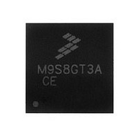
MC9S08GT32ACFDE Freescale, MC9S08GT32ACFDE Datasheet - Page 85

MC9S08GT32ACFDE
Manufacturer Part Number
MC9S08GT32ACFDE
Description
Manufacturer
Freescale
Datasheet
1.MC9S08GT32ACFDE.pdf
(302 pages)
Specifications of MC9S08GT32ACFDE
Cpu Family
HCS08
Device Core Size
8b
Frequency (max)
40MHz
Interface Type
I2C/SCI/SPI
Total Internal Ram Size
2KB
# I/os (max)
39
Number Of Timers - General Purpose
4
Operating Supply Voltage (typ)
2.5/3.3V
Operating Supply Voltage (max)
3.6V
Operating Supply Voltage (min)
1.8/2.08V
On-chip Adc
8-chx10-bit
Instruction Set Architecture
CISC
Operating Temp Range
-40C to 85C
Operating Temperature Classification
Industrial
Mounting
Surface Mount
Pin Count
48
Package Type
QFN EP
Program Memory Type
Flash
Program Memory Size
32KB
Lead Free Status / RoHS Status
Compliant
- Current page: 85 of 302
- Download datasheet (8Mb)
6.3.4
Port D is an 8-bit port shared with the two TPM modules, TPM1 and TPM2, and general-purpose I/O.
When the TPM1 or TPM2 modules are enabled in output compare or input capture modes of operation,
the pin direction will be controlled by the module function.
Port D pins are available as general-purpose I/O pins controlled by the port D data (PTDD), data direction
(PTDDD), pullup enable (PTDPE), and slew rate control (PTDSE) registers. Refer to
I/O
The TPM2 module can be configured to use PTD7–PTD3 as either input capture, output compare, PWM,
or external clock input pins (PTD3 only). Refer to
information about using PTD7–PTD3 as timer pins.
The TPM1 module can be configured to use PTD2–PTD0 as either input capture, output compare, PWM,
or external clock input pins (PTD0 only). Refer to
information about using PTD2–PTD0 as timer pins.
6.3.5
Port E is an 8-bit port shared with the SCI1 module, SPI1 module, and general-purpose I/O. When the SCI
or SPI modules are enabled, the pin direction will be controlled by the module function.
Port E pins are available as general-purpose I/O pins controlled by the port E data (PTED), data direction
(PTEDD), pullup enable (PTEPE), and slew rate control (PTESE) registers. Refer to
I/O
When the SCI1 module is enabled, PTE0 serves as the SCI1 module’s transmit pin (TxD1) and PTE1
serves as the receive pin (RxD1). Refer to
more information about using PTE0 and PTE1 as SCI pins.
When the SPI module is enabled, PTE2 serves as the SPI module’s slave select pin (SS1), PTE3 serves as
the master-in slave-out pin (MISO1), PTE4 serves as the master-out slave-in pin (MOSI1), and PTE5
serves as the SPI clock pin (SPSCK1). Refer to
more information about using PTE5–PTE2 as SPI pins.
Freescale Semiconductor
Controls”
Controls”
Port D
Port E
Port D, TPM1 and TPM2
Port E, SCI1, and SPI
for more information about general-purpose I/O control.
for more information about general-purpose I/O control.
MCU Pin:
MCU Pin:
TPM2CH4
PTD7/
PTE7
Bit 7
Bit 7
TPM2CH3
PTD6/
MC9S08GB60A Data Sheet, Rev. 2
PTE6
Figure 6-5. Port D Pin Names
Figure 6-6. Port E Pin Names
6
6
Chapter 11, “Serial Communications Interface
TPM2CH2
SPSCK1
PTD5/
PTE5/
Chapter 12, “Serial Peripheral Interface (S08SPIV3)
5
5
Chapter 10, “Timer/PWM
Chapter 10, “Timer/PWM
TPM2CH1
MOSI1
PTD4/
PTE4/
4
4
TPM2CH0
MISO1
PTD3/
PTE3/
3
3
TPM1CH2
PTD2/
PTE2/
SS1
2
2
(S08TPMV1)”
(S08TPMV1)”
Chapter 6 Parallel Input/Output
TPM1CH1
PTD1/
PTE1/
RxD1
Section 6.4, “Parallel
Section 6.4, “Parallel
1
1
(S08SCIV1)”
TPM1CH0
PTD0/
PTE0/
TxD1
Bit 0
Bit 0
for more
for more
for
for
85
Related parts for MC9S08GT32ACFDE
Image
Part Number
Description
Manufacturer
Datasheet
Request
R

Part Number:
Description:
TOWER ELEVATOR BOARDS HARDWARE
Manufacturer:
Freescale Semiconductor
Datasheet:

Part Number:
Description:
TOWER SERIAL I/O HARDWARE
Manufacturer:
Freescale Semiconductor
Datasheet:

Part Number:
Description:
LCD MODULE FOR TWR SYSTEM
Manufacturer:
Freescale Semiconductor
Datasheet:

Part Number:
Description:
DAUGHTER LCD WVGA I.MX51
Manufacturer:
Freescale Semiconductor
Datasheet:

Part Number:
Description:
TOWER SYSTEM BOARD MPC5125
Manufacturer:
Freescale Semiconductor
Datasheet:

Part Number:
Description:
KIT EVALUATION I.MX51
Manufacturer:
Freescale Semiconductor
Datasheet:

Part Number:
Description:
KIT DEVELOPMENT WINCE IMX25
Manufacturer:
Freescale Semiconductor
Datasheet:

Part Number:
Description:
TOWER SYSTEM KIT MPC5125
Manufacturer:
Freescale Semiconductor
Datasheet:

Part Number:
Description:
TOWER SYSTEM BOARD K40X256
Manufacturer:
Freescale Semiconductor
Datasheet:

Part Number:
Description:
TOWER SYSTEM KIT K40X256
Manufacturer:
Freescale Semiconductor
Datasheet:

Part Number:
Description:
Microcontrollers (MCU) MX28 PLATFORM DEV KIT
Manufacturer:
Freescale Semiconductor
Datasheet:

Part Number:
Description:
MCU, MPU & DSP Development Tools IAR KickStart Kit for Kinetis K60
Manufacturer:
Freescale Semiconductor
Datasheet:

Part Number:
Description:
24BIT HDMI MX535/08
Manufacturer:
Freescale Semiconductor
Datasheet:
Part Number:
Description:
Manufacturer:
Freescale Semiconductor, Inc
Datasheet:
Part Number:
Description:
Manufacturer:
Freescale Semiconductor, Inc
Datasheet:


