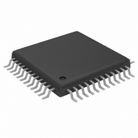
MAX5858AECM+TD Maxim Integrated Products, MAX5858AECM+TD Datasheet - Page 12

MAX5858AECM+TD
Manufacturer Part Number
MAX5858AECM+TD
Description
IC DAC 10BIT DUAL 300MSPS 48TQFP
Manufacturer
Maxim Integrated Products
Datasheet
1.MAX5858AECMD.pdf
(25 pages)
Specifications of MAX5858AECM+TD
Settling Time
11ns
Number Of Bits
10
Data Interface
Parallel
Number Of Converters
2
Voltage Supply Source
Single Supply
Power Dissipation (max)
816mW
Operating Temperature
-40°C ~ 85°C
Mounting Type
Surface Mount
Package / Case
48-TQFP Exposed Pad, 48-eTQFP, 48-HTQFP, 48-VQFP
Lead Free Status / RoHS Status
Lead free / RoHS Compliant
Dual, 10-Bit, 300Msps, DAC with 4x/2x/1x
Interpolation Filters and PLL
12
(AV
differential output, T
6, 19, 47
7, 18, 48
DD
PIN
______________________________________________________________________________________
10
11
12
1
2
3
4
5
8
9
= DV
DD
DA8/DACEN
= PV
DYNAMIC RESPONSE RISE TIME
DA7/F2EN
DA6/F1EN
DA9/PD
DA5/G3
DA4/G2
DA3/G1
DA2/G0
NAME
DGND
DV
A
DA1
DA0
DD
= +25°C, unless otherwise noted.)
DD
= 3V, AGND = DGND = PGND = 0, external reference = 1.2V, no interpolation, PLL disabled, I
10ns/div
Channel A Input Data Bit 9 (MSB)/Power-Down Control Bit:
0: Enter DAC standby mode (DACEN = 0) or power up DAC (DACEN = 1).
1: Enter power-down mode.
Channel A Input Data Bit 8/DAC Enable Control Bit:
0: Enter DAC standby mode with PD = 0.
1: Power up DAC with PD = 0.
X: Enter power-down mode with PD = 1 (X = don’t care.)
Channel A Input Data Bit 7/Second Interpolation Filter Enable Bit:
0: Interpolation mode is determined by F1EN.
1: Enable 4x interpolation mode. (F1EN must equal 1.)
Channel A Input Data Bit 6/First Interpolation Filter Enable Bit:
0: Interpolation disable.
1: Enable 2x interpolation.
Channel A Input Data Bit 5/Channel A Gain Adjustment Bit 3
Digital Ground
Digital Power Supply. See Power Supplies, Bypassing, Decoupling, and Layout section.
Channel A Input Data Bit 4/Channel A Gain Adjustment Bit 2
Channel A Input Data Bit 3/Channel A Gain Adjustment Bit 1
Channel A Input Data Bit 2/Channel A Gain Adjustment Bit 0
Channel A Input Data Bit 1
Channel A Input Data Bit 0 (LSB)
R
SINGLE ENDED
L
= 50Ω
MAX5858A toc33
200mV/div
Typical Operating Characteristics (continued)
FUNCTION
R
SINGLE ENDED
L
DYNAMIC RESPONSE FALL TIME
= 50Ω
10ns/div
Pin Description
MAX5858A toc34
200mV/div
FS
= 20mA,


