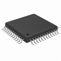
MAX5858AECM+TD Maxim Integrated Products, MAX5858AECM+TD Datasheet - Page 13

MAX5858AECM+TD
Manufacturer Part Number
MAX5858AECM+TD
Description
IC DAC 10BIT DUAL 300MSPS 48TQFP
Manufacturer
Maxim Integrated Products
Datasheet
1.MAX5858AECMD.pdf
(25 pages)
Specifications of MAX5858AECM+TD
Settling Time
11ns
Number Of Bits
10
Data Interface
Parallel
Number Of Converters
2
Voltage Supply Source
Single Supply
Power Dissipation (max)
816mW
Operating Temperature
-40°C ~ 85°C
Mounting Type
Surface Mount
Package / Case
48-TQFP Exposed Pad, 48-eTQFP, 48-HTQFP, 48-VQFP
Lead Free Status / RoHS Status
Lead free / RoHS Compliant
37, 38
40, 46
PIN
13
14
15
16
17
20
21
22
23
24
25
26
27
28
29
30
31
32
33
34
35
36
39
41
42
43
44
45
—
Dual, 10-Bit, 300Msps, DAC with 4x/2x/1x
OUTNB
OUTNA
OUTPB
OUTPA
CLKXP
CLKXN
PLLEN
NAME
AGND
PGND
LOCK
REFO
REFR
AV
PV
PLLF
DB9
DB8
DB7
DB6
DB5
CLK
DB4
DB3
DB2
DB1
DB0
REN
N.C.
IDE
CW
______________________________________________________________________________________
EP
DD
DD
Channel B Input Data Bit 9 (MSB)
Channel B Input Data Bit 8
Channel B Input Data Bit 7
Channel B Input Data Bit 6
Channel B Input Data Bit 5
Clock Output/Input. CLK becomes an input when the PLL is enabled. CLK is an output when the PLL
is disabled.
Interleave Data Mode Enable. When IDE is high, data for both DAC channels is written through port A
(bits DA9–DA0). When IDE is low, channel A data is latched on the rising edge of CLK and channel B
data is latched on the falling edge of CLK.
Channel B Input Data Bit 4
Channel B Input Data Bit 3
Channel B Input Data Bit 2
Channel B Input Data Bit 1
Channel B Input Data Bit 0 (LSB)
Active-Low Control-Word Write Pulse. The control word is latched on the falling edge of CW.
PLL Lock Signal Output. High level indicates that PLL is locked to the CLK signal.
PLL Enabled Input. PLL in enabled when PLLEN is high.
Differential Clock Input Positive Terminal. Connect to PGND when the PLL is enabled. Bypass CLKXP
with a 0.01µF capacitor to PGND when CLKXN is in single-ended mode.
Differential Clock Input Negative Terminal. Connect to PV
with a 0.01µF capacitor to PGND when CLKXP is in single-ended mode.
PLL Power Supply. See Power Supplies, Bypassing, Decoupling, and Layout section.
PLL Ground
PLL Loop Filter. Connect a 4.12kΩ resistor in series with a 100pF capacitor between PLLF and
PGND.
Active-Low Reference Enable. Connect REN to AGND to activate the on-chip 1.24V reference.
Reference I/O. REFO serves as the reference input when the internal reference is disabled. If the
internal 1.24V reference is enabled, REFO serves as the output for the internal reference. When the
internal reference is enabled, bypass REFO to AGND with a 0.1µF capacitor.
No Connection. Not connected internally.
Full-Scale Current Adjustment. To set the output full-scale current, connect an external resistor R
between REFR and AGND. The output full-scale current is equal to 32 × V
Analog Power Supply. See Power Supplies, Bypassing, Decoupling, and Layout section.
Channel B Negative Analog Current Output
Channel B Positive Analog Current Output
Analog Ground
Channel A Negative Analog Current Output
Channel A Positive Analog Current Output
Exposed Paddle. Connect to the ground plane.
Interpolation Filters and PLL
FUNCTION
Pin Description (continued)
DD
when the PLL is enabled. Bypass CLKXN
REFO
/R
SET
.
SET
13


