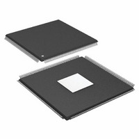
ADSP-21371KSWZ-2B Analog Devices Inc, ADSP-21371KSWZ-2B Datasheet - Page 14

ADSP-21371KSWZ-2B
Manufacturer Part Number
ADSP-21371KSWZ-2B
Description
IC DSP 32BIT 266MHZ 208-LQFP
Manufacturer
Analog Devices Inc
Series
SHARC®r
Type
Floating Pointr
Specifications of ADSP-21371KSWZ-2B
Package / Case
208-LQFP
Interface
DAI, DPI
Operating Temperature
0°C ~ 70°C
Clock Rate
266MHz
Non-volatile Memory
ROM (512 kB)
On-chip Ram
128kB
Voltage - I/o
3.30V
Voltage - Core
1.20V
Mounting Type
Surface Mount
Svhc
No SVHC (18-Jun-2010)
Base Number
21371
Core Frequency Typ
266MHz
Dsp Type
Floating Point
Mmac
532
No. Of Pins
208
Interface Type
SPI, UART
Rohs Compliant
Yes
Operating Temperature Range
0°C To +70°C
Lead Free Status / RoHS Status
Lead free / RoHS Compliant
Available stocks
Company
Part Number
Manufacturer
Quantity
Price
Company:
Part Number:
ADSP-21371KSWZ-2B
Manufacturer:
Analog Devices Inc
Quantity:
10 000
Part Number:
ADSP-21371KSWZ-2B
Manufacturer:
ADI/亚德诺
Quantity:
20 000
ADSP-21371/ADSP-21375
Table 9. Pin Descriptions (Continued)
Name
SDCKE
SDA10
SDCLK
MS
FLAG[0]/IRQ0
FLAG[1]/IRQ1
FLAG[2]/IRQ2/
MS2
FLAG[3]/
TMREXP/ MS3
TDI
TDO
TMS
TCK
TRST
EMU
CLK_CFG
BOOT_CFG
0–1
1–0
1–0
Type
O/T (pu)
O/T (pu)
O/T
O/T (pu)
I/O
I/O
I/O with
programmable pu
(for MS mode)
I/O with
programmable pu
(for MS mode)
I (pu)
O/T
I (pu)
I
I (pu)
O/T (pu)
I
I
State During
and After
Reset
Pulled high/
driven high
Pulled high/
driven low
High-Z/driving
Pulled high/
driven high
FLAG[0] INPUT
FLAG[1] INPUT
FLAG[2] INPUT
FLAG[3] INPUT
Rev. C | Page 14 of 52 | September 2009
Description
SDRAM Clock Enable. Connect to SDRAM’s CKE pin. Enables and disables the CLK
signal. For details, see the data sheet supplied with the SDRAM device.
SDRAM A10 Pin. Enables applications to refresh an SDRAM in parallel with a non-
SDRAM accesses. This pin replaces the DSP’s A10 pin only during SDRAM accesses.
SDRAM Clock.
Memory Select Lines 0–1. These lines are asserted (low) as chip selects for the corre-
sponding banks of external memory. The MS
that change at the same time as the other address lines. When no external memory
access is occurring the MS
tional memory access instruction is executed, whether or not the condition is true.
The MS1 pin can be used in EPORT/FLASH boot mode. For more information, see the
ADSP-2137x SHARC Processor Hardware Reference.
FLAG0/Interrupt Request0.
FLAG1/Interrupt Request1.
FLAG2/Interrupt Request/Memory Select2.
FLAG3/Timer Expired/Memory Select3.
Test Data Input (JTAG). Provides serial data for the boundary scan logic. TDI has a
22.5 k internal pull-up resistor.
Test Data Output (JTAG). Serial scan output of the boundary scan path.
Test Mode Select (JTAG). Used to control the test state machine. TMS has a 22.5 k
internal pull-up resistor.
Test Clock (JTAG). Provides a clock for JTAG boundary scan. TCK must be asserted
(pulsed low) after power-up or held low for proper operation of the processor.
Test Reset (JTAG). Resets the test state machine. TRST must be asserted (pulsed low)
after power-up or held low for proper operation of the processor. TRST has a 22.5 k
internal pull-up resistor.
Emulation Status. Must be connected to the processor. Analog Devices DSP Tools
product line of JTAG emulators target board connector only. EMU has a 22.5 k internal
pull-up resistor.
Core to CLKIN Ratio Control. These pins set the start up clock frequency. See the
ADSP-2137x SHARC Processor Hardware Reference for a description of the clock configu-
ration modes.
Note that the operating frequency can be changed by programming the PLL multiplier
and divider in the PMCTL register at any time after the core comes out of reset.
Boot Configuration Select. These pins select the boot mode for the processor. The
BOOT_CFG pins must be valid before reset is asserted. See the ADSP-2137x SHARC
Processor Hardware Reference for information about boot modes.
3-0
lines are inactive; they are active however when a condi-
3-0
lines are decoded memory address lines


