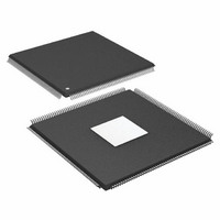
ADSP-21371KSWZ-2B Analog Devices Inc, ADSP-21371KSWZ-2B Datasheet - Page 18

ADSP-21371KSWZ-2B
Manufacturer Part Number
ADSP-21371KSWZ-2B
Description
IC DSP 32BIT 266MHZ 208-LQFP
Manufacturer
Analog Devices Inc
Series
SHARC®r
Type
Floating Pointr
Specifications of ADSP-21371KSWZ-2B
Package / Case
208-LQFP
Interface
DAI, DPI
Operating Temperature
0°C ~ 70°C
Clock Rate
266MHz
Non-volatile Memory
ROM (512 kB)
On-chip Ram
128kB
Voltage - I/o
3.30V
Voltage - Core
1.20V
Mounting Type
Surface Mount
Svhc
No SVHC (18-Jun-2010)
Base Number
21371
Core Frequency Typ
266MHz
Dsp Type
Floating Point
Mmac
532
No. Of Pins
208
Interface Type
SPI, UART
Rohs Compliant
Yes
Operating Temperature Range
0°C To +70°C
Lead Free Status / RoHS Status
Lead free / RoHS Compliant
Available stocks
Company
Part Number
Manufacturer
Quantity
Price
Company:
Part Number:
ADSP-21371KSWZ-2B
Manufacturer:
Analog Devices Inc
Quantity:
10 000
Part Number:
ADSP-21371KSWZ-2B
Manufacturer:
ADI/亚德诺
Quantity:
20 000
ADSP-21371/ADSP-21375
Voltage Controlled Oscillator
In application designs, the PLL multiplier value should be
selected in such a way that the VCO frequency never exceeds
f
The VCO frequency is calculated as follows:
f
f
where:
f
PLLM = Multiplier value programmed in the PMCTL register.
During reset, the PLLM value is derived from the ratio selected
using the CLK_CFG pins in hardware.
PLLD = 1, 2, 4, 8 based on the PLLD value programmed on the
PMCTL register. During reset this value is 1.
f
VCO
VCO
CCLK
VCO
INPUT
• The product of CLKIN and PLLM must never exceed 1/2
• The product of CLKIN and PLLM must never exceed f
f
(INDIV = 0).
(max) in
(INDIV = 1).
= 2
= VCO output
specified in
VCO
= (2
= Input frequency to the PLL.
×
(max) in
RESET
XTAL
×
PLLM
PLLM
Table 14
BUF
Table
×
CLKIN
Table 14
×
f
INPUT
4096 CLKIN
f
DELAY OF
INPUT
CYCLES
if the input divider is enabled
14.
) (2
if the input divider is not enabled
DIVIDER
CLKIN
PMCTL
(INDIV)
×
PLLD)
RESETOUT
f
INPUT
Figure 4. Core Clock and System Clock Relationship to CLKIN
CLK_CFGx/PMCTL (2xPLLM)
Rev. C | Page 18 of 52 | September 2009
FILTER
LOOP
MULTIPLIER
CLKOUT (TEST ONLY)
PLL
VCO
PLL
VCO
f
VCO
f
f
Note the definitions of the clock periods that are a function of
CLKIN and the appropriate ratio control shown in
of the timing specifications for the ADSP-2137x peripherals are
defined in relation to t
for each peripheral’s timing information.
Table 12. Clock Periods
Figure 4
lator or crystal. The shaded divider/multiplier blocks denote
where clock ratios can be set through hardware or software
using the power management control register (PMCTL). For
more information, see the ADSP-2137x SHARC Processor Hard-
ware Reference.
INPUT
INPUT
Timing
Requirements
t
t
t
DIVIDER
(2xPLLD)
CK
CCLK
PCLK
PMCTL
PLL
= CLKIN when the input divider is disabled or
= CLKIN 2 when the input divider is enabled
shows core to CLKIN relationships with external oscil-
f
CCLK
(PLLBP)
PMCTL
CCLK
PCLK
Description
CLKIN Clock Period
Processor Core Clock Period
Peripheral Clock Period = 2 × t
. See the peripheral specific section
(SDCKR)
DIVIDER
SDRAM
PMCTL
DIVIDE
BY 2
BUF
PCLK
CORERST
(PLLBP)
RESETOUT
PMCTL
PCLK
CCLK
SDCLK
Table
CCLK
12. All


