EP3C25F324C8N Altera, EP3C25F324C8N Datasheet - Page 80
EP3C25F324C8N
Manufacturer Part Number
EP3C25F324C8N
Description
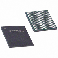
IC CYCLONE III FPGA 25K 324-FBGA
Manufacturer
Altera
Series
Cyclone® IIIr
Datasheets
1.EP3C5F256C8N.pdf
(5 pages)
2.EP3C5F256C8N.pdf
(34 pages)
3.EP3C5F256C8N.pdf
(66 pages)
4.EP3C5F256C8N.pdf
(14 pages)
5.EP3C5F256C8N.pdf
(76 pages)
6.EP3C25F324C8N.pdf
(274 pages)
Specifications of EP3C25F324C8N
Number Of Logic Elements/cells
24624
Number Of Labs/clbs
1539
Total Ram Bits
608256
Number Of I /o
215
Voltage - Supply
1.15 V ~ 1.25 V
Mounting Type
Surface Mount
Operating Temperature
0°C ~ 85°C
Package / Case
324-FBGA
Family Name
Cyclone III
Number Of Logic Blocks/elements
24624
# I/os (max)
215
Frequency (max)
402MHz
Process Technology
65nm
Operating Supply Voltage (typ)
1.2V
Logic Cells
24624
Ram Bits
608256
Operating Supply Voltage (min)
1.15V
Operating Supply Voltage (max)
1.25V
Operating Temp Range
0C to 85C
Operating Temperature Classification
Commercial
Mounting
Surface Mount
Pin Count
324
Package Type
FBGA
For Use With
544-2601 - KIT DEV CYCLONE III LS EP3CLS200544-2411 - KIT DEV NIOS II CYCLONE III ED.544-2370 - KIT STARTER CYCLONE III EP3C25
Lead Free Status / RoHS Status
Lead free / RoHS Compliant
Number Of Gates
-
Lead Free Status / Rohs Status
Compliant
Other names
544-2078
EP3C25F324C8NES
EP3C25F324C8NES
Available stocks
Company
Part Number
Manufacturer
Quantity
Price
Company:

Part Number:
EP3C25F324C8N
Manufacturer:
ALTERA
Quantity:
2 350
Company:
Part Number:
EP3C25F324C8N
Manufacturer:
ALTERA
Quantity:
160
Company:
Part Number:
EP3C25F324C8N
Manufacturer:
ALTERA53
Quantity:
612
Part Number:
EP3C25F324C8N
Manufacturer:
ALTERA/阿尔特拉
Quantity:
20 000
Part Number:
EP3C25F324C8NES
Manufacturer:
ALTERA/阿尔特拉
Quantity:
20 000


5–16
Post-Scale Counter Cascading
Programmable Duty Cycle
Cyclone III Device Handbook, Volume 1
1
Cyclone III device family PLLs support post-scale counter cascading to create
counters larger than 512. This is implemented by feeding the output of one C counter
into the input of the next C counter, as shown in
Figure 5–12. Counter Cascading
When cascading counters to implement a larger division of the high-frequency VCO
clock, the cascaded counters behave as one counter with the product of the individual
counter settings.
For example, if C0 = 4 and C1 = 2, the cascaded value is C0 × C1 = 8.
Post-scale counter cascading is automatically set by the Quartus II software in the
configuration file. Post-scale counter cascading cannot be performed using the PLL
reconfiguration.
The programmable duty cycle allows PLLs to generate clock outputs with a variable
duty cycle. This feature is supported on the PLL post-scale counters. You can achieve
the duty cycle setting by a low and high time count setting for the post-scale counters.
The Quartus II software uses the frequency input and the required multiply or divide
rate to determine the duty cycle choices. The post-scale counter value determines the
precision of the duty cycle. The precision is defined by 50% divided by the post-scale
counter value. For example, if the C0 counter is 10, steps of 5% are possible for duty
cycle choices between 5 to 90%.
Combining the programmable duty cycle with programmable phase shift allows the
generation of precise non-overlapping clocks.
VCO Output
VCO Output
VCO Output
VCO Output
VCO Output
VCO Output
Chapter 5: Clock Networks and PLLs in the Cyclone III Device Family
Figure
C0
C1
C2
C3
C4
5–12.
© December 2009 Altera Corporation
Hardware Features
Related parts for EP3C25F324C8N
Image
Part Number
Description
Manufacturer
Datasheet
Request
R

Part Number:
Description:
CYCLONE II STARTER KIT EP2C20N
Manufacturer:
Altera
Datasheet:


Part Number:
Description:
CPLD, EP610 Family, ECMOS Process, 300 Gates, 16 Macro Cells, 16 Reg., 16 User I/Os, 5V Supply, 35 Speed Grade, 24DIP
Manufacturer:
Altera Corporation
Datasheet:
Part Number:
Description:
CPLD, EP610 Family, ECMOS Process, 300 Gates, 16 Macro Cells, 16 Reg., 16 User I/Os, 5V Supply, 15 Speed Grade, 24DIP
Manufacturer:
Altera Corporation
Datasheet:
Part Number:
Description:
Manufacturer:
Altera Corporation
Datasheet:
Part Number:
Description:
CPLD, EP610 Family, ECMOS Process, 300 Gates, 16 Macro Cells, 16 Reg., 16 User I/Os, 5V Supply, 30 Speed Grade, 24DIP
Manufacturer:
Altera Corporation
Datasheet:
Part Number:
Description:
High-performance, low-power erasable programmable logic devices with 8 macrocells, 10ns
Manufacturer:
Altera Corporation
Datasheet:
Part Number:
Description:
High-performance, low-power erasable programmable logic devices with 8 macrocells, 7ns
Manufacturer:
Altera Corporation
Datasheet:
Part Number:
Description:
Classic EPLD
Manufacturer:
Altera Corporation
Datasheet:
Part Number:
Description:
High-performance, low-power erasable programmable logic devices with 8 macrocells, 10ns
Manufacturer:
Altera Corporation
Datasheet:
Part Number:
Description:
Manufacturer:
Altera Corporation
Datasheet:
Part Number:
Description:
Manufacturer:
Altera Corporation
Datasheet:
Part Number:
Description:
Manufacturer:
Altera Corporation
Datasheet:
Part Number:
Description:
CPLD, EP610 Family, ECMOS Process, 300 Gates, 16 Macro Cells, 16 Reg., 16 User I/Os, 5V Supply, 25 Speed Grade, 24DIP
Manufacturer:
Altera Corporation
Datasheet: