DP83849CVS/NOPB National Semiconductor, DP83849CVS/NOPB Datasheet - Page 13
DP83849CVS/NOPB
Manufacturer Part Number
DP83849CVS/NOPB
Description
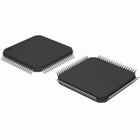
IC TXRX ETHERNET PHY DUAL 80TQFP
Manufacturer
National Semiconductor
Type
Transceiverr
Specifications of DP83849CVS/NOPB
Number Of Drivers/receivers
2/2
Protocol
Ethernet
Voltage - Supply
3 V ~ 3.6 V
Mounting Type
Surface Mount
Package / Case
80-TQFP, 80-VQFP
Data Rate
100Mbps
Supply Voltage Range
3V To 3.6V
Logic Case Style
TQFP
No. Of Pins
80
Operating Temperature Range
0°C To +70°C
Msl
MSL 3 - 168 Hours
Filter Terminals
SMD
Rohs Compliant
Yes
Data Rate Max
10Mbps
For Use With
DP83849CVS-EVK - BOARD EVALUATION DP83849CVS
Lead Free Status / RoHS Status
Lead free / RoHS Compliant
Other names
*DP83849CVS
*DP83849CVS/NOPB
DP83849CVS
*DP83849CVS/NOPB
DP83849CVS
Available stocks
Company
Part Number
Manufacturer
Quantity
Price
Company:

Part Number:
DP83849CVS/NOPB
Manufacturer:
NS
Quantity:
618
Company:
Part Number:
DP83849CVS/NOPB
Manufacturer:
Texas Instruments
Quantity:
10 000


AN_EN
(LED_ACT/LED_COL_A)
AN1_A (LED_SPEED_A)
AN0_A (LED_LINK_A)
AN_EN
(LED_ACT/LED_COL_B)
AN1_B (LED_SPEED_B)
AN0_B (LED_LINK_B)
MII_MODE_A (RX_DV_A)
SNI_MODE_A (TXD3_A)
MII_MODE_B (RX_DV_B)
SNI_MODE_B (TXD3_B)
Signal Name
S, O, PU
S, O, PD
Type
Pin #
21
20
19
41
42
43
80
17
62
45
Auto-Negotiation Enable: When high, this enables Auto-Negoti-
ation with the capability set by AN0 and AN1 pins. When low, this
puts the part into Forced Mode with the capability set by AN0 and
AN1 pins.
AN0 / AN1: These input pins control the forced or advertised op-
erating mode of the DP83849C according to the following table.
The value on these pins is set by connecting the input pins to
GND (0) or V
NEVER be connected directly to GND or VCC.
The value set at this input is latched into the DP83849C at Hard-
ware-Reset.
The float/pull-down status of these pins are latched into the Basic
Mode Control Register and the Auto_Negotiation Advertisement
Register during Hardware-Reset.
The default is 111 since these pins have internal pull-ups.
MII MODE SELECT: This strapping option pair determines the
operating mode of the MAC Data Interface. Default operation
(No pull-ups) will enable normal MII Mode of operation. Strapping
MII_MODE high will cause the device to be in RMII or SNI modes
of operation, determined by the status of the SNI_MODE strap.
Since the pins include internal pull-downs, the default values are
0. Both MAC Data Interfaces must have their RMII Mode settings
the same, i.e. both in RMII mode or both not in RMII mode.
The following table details the configurations:
13
MII_MODE
AN_EN AN1
AN_EN AN1
CC
0
0
0
0
1
1
1
1
(1) through 2.2 k resistors. These pins should
0
1
1
0
0
1
1
0
0
1
1
SNI_MODE
Description
AN0
AN0
0
1
0
1
0
1
0
1
X
0
1
10BASE-T, Half-Duplex
10BASE-T, Full-Duplex
100BASE-TX, Half-Duplex
100BASE-TX, Full-Duplex
10BASE-T, Half/Full-Duplex
100BASE-TX, Half/Full-Duplex
10BASE-T Half-Duplex
100BASE-TX, Half-Duplex
10BASE-T, Half/Full-Duplex
100BASE-TX, Half/Full-Duplex
MII Mode
RMII Mode
10 Mb SNI Mode
Advertised Mode
MAC Interface
Forced Mode
Mode
www.national.com
Related parts for DP83849CVS/NOPB
Image
Part Number
Description
Manufacturer
Datasheet
Request
R

Part Number:
Description:
National Semiconductor [8-Bit D/A Converter]
Manufacturer:
National Semiconductor
Datasheet:
Part Number:
Description:
National Semiconductor [Media Coprocessor]
Manufacturer:
National Semiconductor
Datasheet:
Part Number:
Description:
Digitally Controlled Tone and Volume Circuit with Stereo Audio Power Amplifier, Microphone Preamp Stage and National 3D Sound
Manufacturer:
National Semiconductor
Datasheet:
Part Number:
Description:
Digitally Controlled Tone and Volume Circuit with Stereo Audio Power Amplifier, Microphone Preamp Stage and National 3D Sound
Manufacturer:
National Semiconductor
Datasheet:
Part Number:
Description:
AC97 Rev 2 Codec with Sample Rate Conversion and National 3D Sound
Manufacturer:
National Semiconductor
Part Number:
Description:
Manufacturer:
National Semiconductor
Datasheet:
Part Number:
Description:
Manufacturer:
National Semiconductor
Datasheet:
Part Number:
Description:
General Purpose, Low Voltage, Low Power, Rail-to-Rail Output Operational Amplifiers
Manufacturer:
National Semiconductor
Datasheet:
Part Number:
Description:
8-bit 20 MSPS flash A/D converter.
Manufacturer:
National Semiconductor
Datasheet:
Part Number:
Description:
Low Noise Quad Operational Amplifier
Manufacturer:
National Semiconductor
Datasheet:
Part Number:
Description:
Quad Differential Line Receivers
Manufacturer:
National Semiconductor
Datasheet:
Part Number:
Description:
Quad High Speed Trapezoidal? Bus Transceiver
Manufacturer:
National Semiconductor
Datasheet:
Part Number:
Description:
Dual Line Receiver
Manufacturer:
National Semiconductor
Datasheet:
Part Number:
Description:
TTL to 10k ECL Level Translator with Latch
Manufacturer:
National Semiconductor
Datasheet: