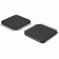
DP83849CVS/NOPB National Semiconductor, DP83849CVS/NOPB Datasheet - Page 25

DP83849CVS/NOPB
Manufacturer Part Number
DP83849CVS/NOPB
Description
IC TXRX ETHERNET PHY DUAL 80TQFP
Manufacturer
National Semiconductor
Type
Transceiverr
Specifications of DP83849CVS/NOPB
Number Of Drivers/receivers
2/2
Protocol
Ethernet
Voltage - Supply
3 V ~ 3.6 V
Mounting Type
Surface Mount
Package / Case
80-TQFP, 80-VQFP
Data Rate
100Mbps
Supply Voltage Range
3V To 3.6V
Logic Case Style
TQFP
No. Of Pins
80
Operating Temperature Range
0°C To +70°C
Msl
MSL 3 - 168 Hours
Filter Terminals
SMD
Rohs Compliant
Yes
Data Rate Max
10Mbps
For Use With
DP83849CVS-EVK - BOARD EVALUATION DP83849CVS
Lead Free Status / RoHS Status
Lead free / RoHS Compliant
Other names
*DP83849CVS
*DP83849CVS/NOPB
DP83849CVS
*DP83849CVS/NOPB
DP83849CVS
Available stocks
Company
Part Number
Manufacturer
Quantity
Price
Company:
Part Number:
DP83849CVS/NOPB
Manufacturer:
NS
Quantity:
618
Company:
Part Number:
DP83849CVS/NOPB
Manufacturer:
Texas Instruments
Quantity:
10 000
3.4.3 Serial Management Preamble Suppression
The DP83849C supports a Preamble Suppression mode
as indicated by a one in bit 6 of the Basic Mode Status
Register (BMSR, address 01h.) If the station management
entity (i.e. MAC or other management controller) deter-
mines that all PHYs in the system support Preamble Sup-
pression by returning a one in this bit, then the station
management entity need not generate preamble for each
management transaction.
The DP83849C requires a single initialization sequence of
32 bits of preamble following hardware/software reset. This
requirement is generally met by the mandatory pull-up
resistor on MDIO in conjunction with a continuous MDC, or
the management access made to determine whether Pre-
amble Suppression is supported.
Read Operation
Write Operation
MII Management
MDIO
MDIO
MDC
MDC
MDIO
Serial Protocol
(STA)
(PHY)
(STA)
Z
Idle
Z
Idle
Z
Z
0
0
Start
Start
1 1
1
Opcode
(Read)
Opcode
(Write)
0
0 0
1
0
(PHYAD = 0Ch)
(PHYAD = 0Ch)
PHY Address
PHY Address
1 1 0 0 0 0 0 0 0
1 1 0 0 0 0 0 0 0
<idle><start><op code><device addr><reg addr><turnaround><data><idle>
Figure 5. Typical MDC/MDIO Write Operation
Figure 4. Typical MDC/MDIO Read Operation
<idle><01><10><AAAAA><RRRRR><Z0><xxxx xxxx xxxx xxxx><idle>
<idle><01><01><AAAAA><RRRRR><10><xxxx xxxx xxxx xxxx><idle>
Table 5. Typical MDIO Frame Format
Register Address
Register Address
(00h = BMCR)
(00h = BMCR)
Z
Z
Z
25
1
TA
0 0 0 1 1 0 0 0 1 0 0 0 0 0 0 0 0
TA
While the DP83849C requires an initial preamble
sequence of 32 bits for management initialization, it does
not require a full 32-bit sequence between each subse-
quent transaction. A minimum of one idle bit between man-
agement transactions is required as specified in the IEEE
802.3u specification.
3.4.4 Simultaneous Register Write
The DP83849C incorporates a mode which allows simulta-
neous write access to both Port A and B register blocks at
the same time. This mode is selected by setting bit 15 of
RMII and Bypass Register (RBR, address 17h) in Port A.
As long as this bit remains set, subsequent writes to Port A
will write to registers in both ports. Register reads are unaf-
fected. Each port must still be read individually.
0 0 0
0 0
0 0 0
Register Data
Register Data
0
0 0 0 0 0 0 0 0
www.national.com
Z
Idle
Z
Z
Idle
Z


