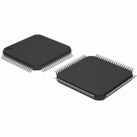
DP83849CVS/NOPB National Semiconductor, DP83849CVS/NOPB Datasheet - Page 20

DP83849CVS/NOPB
Manufacturer Part Number
DP83849CVS/NOPB
Description
IC TXRX ETHERNET PHY DUAL 80TQFP
Manufacturer
National Semiconductor
Type
Transceiverr
Specifications of DP83849CVS/NOPB
Number Of Drivers/receivers
2/2
Protocol
Ethernet
Voltage - Supply
3 V ~ 3.6 V
Mounting Type
Surface Mount
Package / Case
80-TQFP, 80-VQFP
Data Rate
100Mbps
Supply Voltage Range
3V To 3.6V
Logic Case Style
TQFP
No. Of Pins
80
Operating Temperature Range
0°C To +70°C
Msl
MSL 3 - 168 Hours
Filter Terminals
SMD
Rohs Compliant
Yes
Data Rate Max
10Mbps
For Use With
DP83849CVS-EVK - BOARD EVALUATION DP83849CVS
Lead Free Status / RoHS Status
Lead free / RoHS Compliant
Other names
*DP83849CVS
*DP83849CVS/NOPB
DP83849CVS
*DP83849CVS/NOPB
DP83849CVS
Available stocks
Company
Part Number
Manufacturer
Quantity
Price
Company:
Part Number:
DP83849CVS/NOPB
Manufacturer:
NS
Quantity:
618
Company:
Part Number:
DP83849CVS/NOPB
Manufacturer:
Texas Instruments
Quantity:
10 000
www.national.com
2.4 LED Interface
The DP83849C supports three configurable Light Emitting
Diode (LED) pins for each port.
Several functions can be multiplexed onto the three LEDs
using three different modes of operation. The LED opera-
tion mode can be selected by writing to the LED_CFG[1:0]
The LED_LINK pin in Mode 1 indicates the link status of
the port. In 100BASE-T mode, link is established as a
result of input receive amplitude compliant with the TP-
PMD specifications which will result in internal generation
of signal detect. A 10 Mb/s Link is established as a result of
the reception of at least seven consecutive normal Link
Pulses or the reception of a valid 10BASE-T packet. This
will cause the assertion of LED_LINK. LED_LINK will deas-
sert in accordance with the Link Loss Timer as specified in
the IEEE 802.3 specification.
The LED_LINK pin in Mode 1 will be OFF when no LINK is
present.
The LED_LINK pin in Mode 2 and Mode 3 will be ON to
indicate Link is good and BLINK to indicate activity is
present on activity. The BLINK frequency is defined in
BLINK_FREQ, bits [7:6] of register LEDCR (18h).
Activity is defined as configured in LEDACT_RX, bit 8 of
register LEDCR (18h). If LEDACT_RX is 0, Activity is sig-
naled for either transmit or receive. If LEDACT_RX is 1,
Activity is only signaled for receive.
The LED_SPEED pin indicates 10 or 100 Mb/s data rate of
the port. The LED is ON when operating in 100Mb/s mode
and OFF when operating in 10Mb/s mode. The functional-
ity of this LED is independent of mode selected.
The LED_ACT/LED_COL pin in Mode 1 indicates the pres-
ence of either transmit or receive activity. The LED will be
ON for Activity and OFF for No Activity. In Mode 2, this pin
indicates the Collision status of the port. The LED will be
ON for Collision and OFF for No Collision.
Mode
1
2
3
LED_CFG[1]
don’t care
0
1
LED_CFG[0]
1
0
0
ON for Good Link
OFF for No Link
ON for Good Link
BLINK for Activity
ON for Good Link
BLINK for Activity
Table 3. LED Mode Select
LED_LINK
20
register bits in the PHY Control Register (PHYCR) at
address 19h, bits [6:5]. In addition, LED_CFG[0] for each
port can be set by a strap option on the CRS_A and
CRS_B pins. LED_CFG[1] is only controllable through reg-
ister access and cannot be set by as strap pin.
See Table 3 for LED Mode selection.
The LED_ACT/LED_COL pin in Mode 3 indicates Duplex
status for 10 Mb/s or 100 Mb/s operation. The LED will be
ON for Full Duplex and OFF for Half Duplex.
In 10 Mb/s half duplex mode, the collision LED is based on
the COL signal.
Since these LED pins are also used as strap options, the
polarity of the LED is dependent on whether the pin is
pulled up or down.
2.4.1 LEDs
Since the Auto-Negotiation (AN) strap options share the
LED output pins, the external components required for
strapping and LED usage must be considered in order to
avoid contention.
Specifically, when the LED outputs are used to drive LEDs
directly, the active state of each output driver is dependent
on the logic level sampled by the corresponding AN input
upon power-up/reset. For example, if a given AN input is
resistively pulled low then the corresponding output will be
configured as an active high driver. Conversely, if a given
AN input is resistively pulled high, then the corresponding
output will be configured as an active low driver.
Refer to Figure 3 for an example of AN connections to
external components at port A. In this example, the AN
strapping results in Auto-Negotiation disabled with 100
Full-Duplex forced.
The adaptive nature of the LED outputs helps to simplify
potential implementation issues of these dual purpose pins.
ON in 100 Mb/s
OFF in 10 Mb/s
ON in 100 Mb/s
OFF in 10 Mb/s
ON in 100 Mb/s
OFF in 10 Mb/s
LED_SPEED
ON for Activity
OFF for No Activity
ON for Collision
OFF for No Collision
ON for Full Duplex
OFF for Half Duplex
LED_ACT/LED_COL


