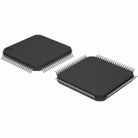
DP83849CVS/NOPB National Semiconductor, DP83849CVS/NOPB Datasheet - Page 31

DP83849CVS/NOPB
Manufacturer Part Number
DP83849CVS/NOPB
Description
IC TXRX ETHERNET PHY DUAL 80TQFP
Manufacturer
National Semiconductor
Type
Transceiverr
Specifications of DP83849CVS/NOPB
Number Of Drivers/receivers
2/2
Protocol
Ethernet
Voltage - Supply
3 V ~ 3.6 V
Mounting Type
Surface Mount
Package / Case
80-TQFP, 80-VQFP
Data Rate
100Mbps
Supply Voltage Range
3V To 3.6V
Logic Case Style
TQFP
No. Of Pins
80
Operating Temperature Range
0°C To +70°C
Msl
MSL 3 - 168 Hours
Filter Terminals
SMD
Rohs Compliant
Yes
Data Rate Max
10Mbps
For Use With
DP83849CVS-EVK - BOARD EVALUATION DP83849CVS
Lead Free Status / RoHS Status
Lead free / RoHS Compliant
Other names
*DP83849CVS
*DP83849CVS/NOPB
DP83849CVS
*DP83849CVS/NOPB
DP83849CVS
Available stocks
Company
Part Number
Manufacturer
Quantity
Price
Company:
Part Number:
DP83849CVS/NOPB
Manufacturer:
NS
Quantity:
618
Company:
Part Number:
DP83849CVS/NOPB
Manufacturer:
Texas Instruments
Quantity:
10 000
4.2.2.2 Base Line Wander Compensation
The DP83849C is completely ANSI TP-PMD compliant and
includes Base Line Wander (BLW) compensation. The
BLW compensation block can successfully recover the TP-
PMD defined “killer” pattern.
BLW can generally be defined as the change in the aver-
age DC content, relatively short period over time, of an AC
coupled digital transmission over a given transmission
medium. (i.e., copper wire).
BLW results from the interaction between the low fre-
quency components of a transmitted bit stream and the fre-
quency response of the AC coupling component(s) within
the transmission system. If the low frequency content of
the digital bit stream goes below the low frequency pole of
the AC coupling transformers then the droop characteris-
tics of the transformers will dominate resulting in potentially
serious BLW.
The digital oscilloscope plot provided in Figure 10 illus-
trates the severity of the BLW event that can theoretically
be generated during 100BASE-TX packet transmission.
This event consists of approximately 800 mV of DC offset
for a period of 120 s. Left uncompensated, events such as
this can cause packet loss.
4.2.3 Signal Detect
The signal detect function of the DP83849C is incorporated
to meet the specifications mandated by the ANSI FDDI TP-
Figure 10. 100BASE-TX BLW Event
31
PMD Standard as well as the IEEE 802.3 100BASE-TX
Standard for both voltage thresholds and timing parame-
ters.
Note that the reception of normal 10BASE-T link pulses
and fast link pulses per IEEE 802.3u Auto-Negotiation by
the 100BASE-TX receiver do not cause the DP83849C to
assert signal detect.
4.2.4 MLT-3 to NRZI Decoder
The DP83849C decodes the MLT-3 information from the
Digital Adaptive Equalizer block to binary NRZI data.
4.2.5 NRZI to NRZ
In a typical application, the NRZI to NRZ decoder is
required in order to present NRZ formatted data to the
descrambler.
4.2.6 Serial to Parallel
The 100BASE-TX receiver includes a Serial to Parallel
converter which supplies 5-bit wide data symbols to the
PCS Rx state machine.
www.national.com


