Si5369-EVB Silicon Laboratories Inc, Si5369-EVB Datasheet - Page 10
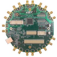
Si5369-EVB
Manufacturer Part Number
Si5369-EVB
Description
MCU, MPU & DSP Development Tools SI5369 DEV KIT
Manufacturer
Silicon Laboratories Inc
Specifications of Si5369-EVB
Processor To Be Evaluated
Si5369
Interface Type
I2C, SPI
Operating Supply Voltage
3.3 V
Lead Free Status / Rohs Status
Details


10
Table 4. AC Specifications
(V
Single-Ended Reference Clock Input Pin XA (XB with cap to GND)
Input Resistance
Input Voltage Swing
Differential Reference Clock Input Pins (XA/XB)
Input Voltage Swing
CKINn Input Pins
Input Frequency
Input Duty Cycle
(Minimum Pulse
Width)
Input Capacitance
Input Rise/Fall Time
CKOUTn Output Pins
(See ordering section for speed grade vs frequency limits)
Output Frequency
(Output not config-
ured for CMOS or
Disabled)
Maximum Output
Frequency in CMOS
Format
Output Rise/Fall
(20–80 %) @
622.08 MHz output
Output Rise/Fall
(20–80%) @
212.5 MHz output
*Note: Input to output phase skew after an ICAL is not controlled and can assume any value.
DD
= 1.8 ± 5%, 2.5 ±10%, or 3.3 V ±10%, T
Parameter
XA/XB
CKO
CKO
Symbol
CKN
CKN
CKN
XA
XA
CKN
CKO
CKO
VPP
RIN
TRF
TRF
TRF
CIN
DC
VPP
F
F
F
Output not configured for
A
RATE[1:0] = LM, MH,
RATE[1:0] = LM, MH,
limitation applies only
RATE[1:0] = LM, MH
Whichever is smaller
= –40 to 85 °C)
(i.e., the 40% / 60%
CMOS or Disabled
to high frequency
Test Condition
CMOS Output
C
See Figure 2
See Figure 2
V
ac coupled
ac coupled
LOAD
Preliminary Rev. 0.4
20–80%
DD
clocks)
N1 = 5
N1 = 4
N1 6
= 1.71
= 5 pF
1.213
0.002
0.002
Min
970
0.5
0.5
40
—
—
—
—
—
—
2
Typ
230
12
—
—
—
—
—
—
—
—
—
—
—
—
212.5
1134
Max
710
945
350
1.2
2.4
1.4
—
60
—
11
3
8
MHz
MHz
MHz
MHz
Unit
GHz
V
V
k
pF
ns
ns
ps
ns
%
PP
PP
Related parts for Si5369-EVB
Image
Part Number
Description
Manufacturer
Datasheet
Request
R

Part Number:
Description:
SMD/C°/SINGLE-ENDED OUTPUT SILICON OSCILLATOR
Manufacturer:
Silicon Laboratories Inc
Part Number:
Description:
Manufacturer:
Silicon Laboratories Inc
Datasheet:
Part Number:
Description:
N/A N/A/SI4010 AES KEYFOB DEMO WITH LCD RX
Manufacturer:
Silicon Laboratories Inc
Datasheet:
Part Number:
Description:
N/A N/A/SI4010 SIMPLIFIED KEY FOB DEMO WITH LED RX
Manufacturer:
Silicon Laboratories Inc
Datasheet:
Part Number:
Description:
N/A/-40 TO 85 OC/EZLINK MODULE; F930/4432 HIGH BAND (REV E/B1)
Manufacturer:
Silicon Laboratories Inc
Part Number:
Description:
EZLink Module; F930/4432 Low Band (rev e/B1)
Manufacturer:
Silicon Laboratories Inc
Part Number:
Description:
I°/4460 10 DBM RADIO TEST CARD 434 MHZ
Manufacturer:
Silicon Laboratories Inc
Part Number:
Description:
I°/4461 14 DBM RADIO TEST CARD 868 MHZ
Manufacturer:
Silicon Laboratories Inc
Part Number:
Description:
I°/4463 20 DBM RFSWITCH RADIO TEST CARD 460 MHZ
Manufacturer:
Silicon Laboratories Inc
Part Number:
Description:
I°/4463 20 DBM RADIO TEST CARD 868 MHZ
Manufacturer:
Silicon Laboratories Inc
Part Number:
Description:
I°/4463 27 DBM RADIO TEST CARD 868 MHZ
Manufacturer:
Silicon Laboratories Inc
Part Number:
Description:
I°/4463 SKYWORKS 30 DBM RADIO TEST CARD 915 MHZ
Manufacturer:
Silicon Laboratories Inc
Part Number:
Description:
N/A N/A/-40 TO 85 OC/4463 RFMD 30 DBM RADIO TEST CARD 915 MHZ
Manufacturer:
Silicon Laboratories Inc
Part Number:
Description:
I°/4463 20 DBM RADIO TEST CARD 169 MHZ
Manufacturer:
Silicon Laboratories Inc