Si5369-EVB Silicon Laboratories Inc, Si5369-EVB Datasheet - Page 9
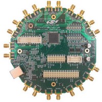
Si5369-EVB
Manufacturer Part Number
Si5369-EVB
Description
MCU, MPU & DSP Development Tools SI5369 DEV KIT
Manufacturer
Silicon Laboratories Inc
Specifications of Si5369-EVB
Processor To Be Evaluated
Si5369
Interface Type
I2C, SPI
Operating Supply Voltage
3.3 V
Lead Free Status / Rohs Status
Details


Table 3. DC Characteristics (Continued)
(V
3-Level Input Pins
Input Voltage Low
Input Voltage Mid
Input Voltage High
Input Low Current
Input Mid Current
Input High Current
LVCMOS Output Pins
Output Voltage Low
Output Voltage Low
Output Voltage High
Output Voltage High
Disabled Leakage
Current
Notes:
DD
1. Current draw is independent of supply voltage
2. No under- or overshoot is allowed.
3. LVPECL outputs require nominal VDD ≥ 2.5 V.
4. This is the amount of leakage that the 3-Level inputs can tolerate from an external driver. See Si53xx Family Reference
5. LVPECL, CML, LVDS and low-swing LVDS measured with Fo = 622.08 MHz.
6. The LVPECL and CMOS output formats draw more current than either LVDS or CML; however, there are restrictions in
= 1.8 ± 5%, 2.5 ±10%, or 3.3 V ±10%, T
Parameter
Manual for more details.
the allowed output format pin settings so that the maximum power dissipation for the TQFP devices is limited when
they are operated at 3.3 V. When there are four enabled LVPECL or CMOS outputs, the fifth output must be disabled.
When there are five enabled outputs, there can be no more than three outputs that are either LVPECL or CMOS.
4
Symbol
V
V
I
V
V
V
I
I
I
IMM
IHH
IMM
ILL
OZ
IHH
ILL
OH
OL
A
= –40 to 85 °C)
Test Condition
V
V
V
V
IO = –2 mA
See Note 4
See Note 4
See Note 4
IO = –2 mA
IO = 2 mA
DD
IO = 2 mA
DD
DD
DD
Preliminary Rev. 0.4
RSTb = 0
= 1.71 V
= 2.97 V
= 1.71 V
= 2.97 V
0.45 x
0.85 x
V
V
–100
V
V
Min
–20
DD
0.4
DD
0.4
–2
—
—
—
—
DD
DD
–
–
Typ
—
—
—
—
—
—
—
—
—
—
—
0.15 x V
0.55 x V
Max
100
0.4
0.4
+2
20
—
—
—
—
DD
DD
Unit
µA
µA
µA
µA
V
V
V
V
V
V
V
9
Related parts for Si5369-EVB
Image
Part Number
Description
Manufacturer
Datasheet
Request
R

Part Number:
Description:
SMD/C°/SINGLE-ENDED OUTPUT SILICON OSCILLATOR
Manufacturer:
Silicon Laboratories Inc
Part Number:
Description:
Manufacturer:
Silicon Laboratories Inc
Datasheet:
Part Number:
Description:
N/A N/A/SI4010 AES KEYFOB DEMO WITH LCD RX
Manufacturer:
Silicon Laboratories Inc
Datasheet:
Part Number:
Description:
N/A N/A/SI4010 SIMPLIFIED KEY FOB DEMO WITH LED RX
Manufacturer:
Silicon Laboratories Inc
Datasheet:
Part Number:
Description:
N/A/-40 TO 85 OC/EZLINK MODULE; F930/4432 HIGH BAND (REV E/B1)
Manufacturer:
Silicon Laboratories Inc
Part Number:
Description:
EZLink Module; F930/4432 Low Band (rev e/B1)
Manufacturer:
Silicon Laboratories Inc
Part Number:
Description:
I°/4460 10 DBM RADIO TEST CARD 434 MHZ
Manufacturer:
Silicon Laboratories Inc
Part Number:
Description:
I°/4461 14 DBM RADIO TEST CARD 868 MHZ
Manufacturer:
Silicon Laboratories Inc
Part Number:
Description:
I°/4463 20 DBM RFSWITCH RADIO TEST CARD 460 MHZ
Manufacturer:
Silicon Laboratories Inc
Part Number:
Description:
I°/4463 20 DBM RADIO TEST CARD 868 MHZ
Manufacturer:
Silicon Laboratories Inc
Part Number:
Description:
I°/4463 27 DBM RADIO TEST CARD 868 MHZ
Manufacturer:
Silicon Laboratories Inc
Part Number:
Description:
I°/4463 SKYWORKS 30 DBM RADIO TEST CARD 915 MHZ
Manufacturer:
Silicon Laboratories Inc
Part Number:
Description:
N/A N/A/-40 TO 85 OC/4463 RFMD 30 DBM RADIO TEST CARD 915 MHZ
Manufacturer:
Silicon Laboratories Inc
Part Number:
Description:
I°/4463 20 DBM RADIO TEST CARD 169 MHZ
Manufacturer:
Silicon Laboratories Inc