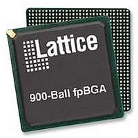
LFE2M70E-5FN900C Lattice, LFE2M70E-5FN900C Datasheet - Page 13

LFE2M70E-5FN900C
Manufacturer Part Number
LFE2M70E-5FN900C
Description
IC, LATTICEECP2M FPGA, 420MHZ, FPBGA-900
Manufacturer
Lattice
Series
LatticeECP2Mr
Datasheet
1.LFE2-12E-5FN256C.pdf
(385 pages)
Specifications of LFE2M70E-5FN900C
No. Of Logic Blocks
67000
No. Of Macrocells
34000
No. Of Speed Grades
5
Total Ram Bits
4534Kbit
No. Of I/o's
416
Clock Management
DLL, PLL
I/o Supply Voltage
3.465V
Rohs Compliant
Yes
Lead Free Status / Rohs Status
Lead free / RoHS Compliant
Available stocks
Company
Part Number
Manufacturer
Quantity
Price
Company:
Part Number:
LFE2M70E-5FN900C
Manufacturer:
Lattice Semiconductor Corporation
Quantity:
10 000
- Current page: 13 of 385
- Download datasheet (3Mb)
Lattice Semiconductor
The DLLs in the LatticeECP2/M are used to shift the clock in relation to the data for source synchronous inputs.
PLLs are used for frequency synthesis and clock generation for source synchronous interfaces. Cascading PLL
and DLL blocks allows applications to utilize the unique benefits of both DLLs and PLLs.
For further information about the DLL, please see the list of additional technical documentation at the end of this
data sheet.
GPLL/SPLL/GDLL PIO Input Pin Connections (LatticeECP2M Family Only)
All LatticeECP2M devices contain two GDLLs, two GPLLs and six SPLLs, arranged in quadrants as shown in
Figure 2-8. In the LatticeECP2M devices GPLLs, SPLLs and GDLLs share their input pins. Figure 2-8 shows the
sharing of SPLLs input pin connections in the upper two quadrants and the sharing of GDLL, GPLL and SPLL input
pin connections in the lower two quadrants.
Figure 2-8. Sharing of PIO Pins by GPLL, SPLL and GDLL in LatticeECP2M Devices
Clock Dividers
LatticeECP2/M devices have two clock dividers, one on the left side and one on the right side of the device. These
are intended to generate a slower-speed system clock from a high-speed edge clock. The block operates in a ÷2,
÷4 or ÷8 mode and maintains a known phase relationship between the divided down clock and the high-speed
clock based on the release of its reset signal. The clock dividers can be fed from selected PLL/DLL outputs, DLL-
DELA delay blocks, routing or from an external clock input. The clock divider outputs serve as primary clock
sources and feed into the clock distribution network. The Reset (RST) control signal resets input and synchro-
nously forces all outputs to low. The RELEASE signal releases outputs synchronously to the input clock. For further
information about clock dividers, please see the list of additional technical documentation at the end of this data
sheet. Figure 2-9 shows the clock divider connections.
GPLL_PIO
GDLL_PIO
SPLL_PIO
SPLL_PIO
SPLL_PIO
Upper Left Quadrant
Lower Left Quadrant
GPLL
GDLL
SPLL
SPLL
SPLL
2-10
Upper Right Quadrant
Lower Right Quadrant
GPLL
GDLL
SPLL
SPLL
SPLL
LatticeECP2/M Family Data Sheet
GDLL_PIO
SPLL_PIO
SPLL_PIO
SPLL_PIO
GPLL_PIO
Architecture
Related parts for LFE2M70E-5FN900C
Image
Part Number
Description
Manufacturer
Datasheet
Request
R
Part Number:
Description:
Manufacturer:
Lattice Semiconductor Corp.
Datasheet:
Part Number:
Description:
IC, LATTICEECP2M FPGA, 420MHZ, FPBGA-900
Manufacturer:
LATTICE SEMICONDUCTOR
Datasheet:

Part Number:
Description:
IC FPGA 50KLUTS 410I/O 900-BGA
Manufacturer:
Lattice
Datasheet:

Part Number:
Description:
IC FPGA 50KLUTS 410I/O 900-BGA
Manufacturer:
Lattice
Datasheet:

Part Number:
Description:
IC FPGA 67KLUTS 1152FPBGA
Manufacturer:
Lattice
Datasheet:

Part Number:
Description:
IC FPGA 67KLUTS 900FPBGA
Manufacturer:
Lattice
Datasheet:

Part Number:
Description:
IC FPGA 67KLUTS 1152FPBGA
Manufacturer:
Lattice
Datasheet:

Part Number:
Description:
IC FPGA 67KLUTS 1152FPBGA
Manufacturer:
Lattice
Datasheet:

Part Number:
Description:
IC FPGA 67KLUTS 1152FPBGA
Manufacturer:
Lattice
Datasheet:

Part Number:
Description:
FPGA - Field Programmable Gate Array 67K LUTs 430 I/O Memry DSP 1.2V -5Spd
Manufacturer:
Lattice

Part Number:
Description:
FPGA - Field Programmable Gate Array 67K LUTs 430 I/O Memry DSP 1.2V -7Spd
Manufacturer:
Lattice

Part Number:
Description:
FPGA - Field Programmable Gate Array 67K LUTs 430 I/O Memry DSP 1.2V -5Spd
Manufacturer:
Lattice

Part Number:
Description:
FPGA - Field Programmable Gate Array 67K LUTs 430 I/O Memry DSP 1.2V -6Spd
Manufacturer:
Lattice

Part Number:
Description:
FPGA - Field Programmable Gate Array 67K LUTs 416 I/O Memory DSP 1.2V 5SPD
Manufacturer:
Lattice


