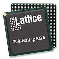
LFE2M70E-5FN900C Lattice, LFE2M70E-5FN900C Datasheet - Page 20

LFE2M70E-5FN900C
Manufacturer Part Number
LFE2M70E-5FN900C
Description
IC, LATTICEECP2M FPGA, 420MHZ, FPBGA-900
Manufacturer
Lattice
Series
LatticeECP2Mr
Datasheet
1.LFE2-12E-5FN256C.pdf
(385 pages)
Specifications of LFE2M70E-5FN900C
No. Of Logic Blocks
67000
No. Of Macrocells
34000
No. Of Speed Grades
5
Total Ram Bits
4534Kbit
No. Of I/o's
416
Clock Management
DLL, PLL
I/o Supply Voltage
3.465V
Rohs Compliant
Yes
Lead Free Status / Rohs Status
Lead free / RoHS Compliant
Available stocks
Company
Part Number
Manufacturer
Quantity
Price
Company:
Part Number:
LFE2M70E-5FN900C
Manufacturer:
Lattice Semiconductor Corporation
Quantity:
10 000
- Current page: 20 of 385
- Download datasheet (3Mb)
Lattice Semiconductor
Slice Clock Selection
Figure 2-17 shows the clock selections and Figure 2-18 shows the control selections for Slice0 through Slice2. All
the primary clocks and the four secondary clocks are routed to this clock selection mux. Other signals can be used
as a clock input to the slices via routing. Slice controls are generated from the secondary clocks or other signals
connected via routing.
If none of the signals are selected for both clock and control then the default value of the mux output is 1. Slice 3
does not have any registers; therefore it does not have the clock or control muxes.
Figure 2-17. Slice0 through Slice2 Clock Selection
Figure 2-18. Slice0 through Slice2 Control Selection
Edge Clock Routing
LatticeECP2/M devices have a number of high-speed edge clocks that are intended for use with the PIOs in the
implementation of high-speed interfaces. There are eight edge clocks per device: two edge clocks per edge. Differ-
ent PLL and DLL outputs are routed to the two muxes on the left and right sides of the device. In addition, the
CLKO signal (generated from the DLLDELA block) is routed to all the edge clock muxes on the left and right sides
of the device. Figure 2-19 shows the selection muxes for these clocks.
Secondary Clock
Secondary Clock
Primary Clock
Routing
Routing
Vcc
Vcc
12
12
8
4
1
3
1
2-17
25:1
16:1
LatticeECP2/M Family Data Sheet
Clock to Slice
Slice Control
Architecture
Related parts for LFE2M70E-5FN900C
Image
Part Number
Description
Manufacturer
Datasheet
Request
R
Part Number:
Description:
Manufacturer:
Lattice Semiconductor Corp.
Datasheet:
Part Number:
Description:
IC, LATTICEECP2M FPGA, 420MHZ, FPBGA-900
Manufacturer:
LATTICE SEMICONDUCTOR
Datasheet:

Part Number:
Description:
IC FPGA 50KLUTS 410I/O 900-BGA
Manufacturer:
Lattice
Datasheet:

Part Number:
Description:
IC FPGA 50KLUTS 410I/O 900-BGA
Manufacturer:
Lattice
Datasheet:

Part Number:
Description:
IC FPGA 67KLUTS 1152FPBGA
Manufacturer:
Lattice
Datasheet:

Part Number:
Description:
IC FPGA 67KLUTS 900FPBGA
Manufacturer:
Lattice
Datasheet:

Part Number:
Description:
IC FPGA 67KLUTS 1152FPBGA
Manufacturer:
Lattice
Datasheet:

Part Number:
Description:
IC FPGA 67KLUTS 1152FPBGA
Manufacturer:
Lattice
Datasheet:

Part Number:
Description:
IC FPGA 67KLUTS 1152FPBGA
Manufacturer:
Lattice
Datasheet:

Part Number:
Description:
FPGA - Field Programmable Gate Array 67K LUTs 430 I/O Memry DSP 1.2V -5Spd
Manufacturer:
Lattice

Part Number:
Description:
FPGA - Field Programmable Gate Array 67K LUTs 430 I/O Memry DSP 1.2V -7Spd
Manufacturer:
Lattice

Part Number:
Description:
FPGA - Field Programmable Gate Array 67K LUTs 430 I/O Memry DSP 1.2V -5Spd
Manufacturer:
Lattice

Part Number:
Description:
FPGA - Field Programmable Gate Array 67K LUTs 430 I/O Memry DSP 1.2V -6Spd
Manufacturer:
Lattice

Part Number:
Description:
FPGA - Field Programmable Gate Array 67K LUTs 416 I/O Memory DSP 1.2V 5SPD
Manufacturer:
Lattice


