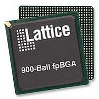
LFE2M70E-5FN900C Lattice, LFE2M70E-5FN900C Datasheet - Page 51

LFE2M70E-5FN900C
Manufacturer Part Number
LFE2M70E-5FN900C
Description
IC, LATTICEECP2M FPGA, 420MHZ, FPBGA-900
Manufacturer
Lattice
Series
LatticeECP2Mr
Datasheet
1.LFE2-12E-5FN256C.pdf
(385 pages)
Specifications of LFE2M70E-5FN900C
No. Of Logic Blocks
67000
No. Of Macrocells
34000
No. Of Speed Grades
5
Total Ram Bits
4534Kbit
No. Of I/o's
416
Clock Management
DLL, PLL
I/o Supply Voltage
3.465V
Rohs Compliant
Yes
Lead Free Status / Rohs Status
Lead free / RoHS Compliant
Available stocks
Company
Part Number
Manufacturer
Quantity
Price
Company:
Part Number:
LFE2M70E-5FN900C
Manufacturer:
Lattice Semiconductor Corporation
Quantity:
10 000
- Current page: 51 of 385
- Download datasheet (3Mb)
Lattice Semiconductor
for checking soft errors (SED) in SRAM. This SED operation can be run in the background during user mode. If a
soft error occurs, during user mode (normal operation) the device can be programmed to either reload from a
known good boot image or generate an error signal.
For further information about Soft Error Detect (SED) support, please see the list of additional technical documen-
tation at the end of this data sheet.
External Resistor
LatticeECP2/M devices require a single external, 10K ohm ±1% value between the XRES pin and ground. Device
configuration will not be completed if this resistor is missing. There is no boundary scan register on the external
resistor pad.
On-Chip Oscillator
Every LatticeECP2/M device has an internal CMOS oscillator which is used to derive a Master Clock for configura-
tion. The oscillator and the Master Clock run continuously and are available to user logic after configuration is com-
pleted. The software default value of the Master Clock is 2.5MHz. Table 2-16 lists all the available Master
Configuration Clock frequencies for normal non-encrypted mode and encrypted mode. When a different Master
Clock is selected during the design process, the following sequence takes place:
1. Device powers up with a Master Clock frequency of 3.1MHz.
2. During configuration, users select a different master clock frequency.
3. The Master Clock frequency changes to the selected frequency once the clock configuration bits are received.
4. If the user does not select a master clock frequency, then the configuration bitstream defaults to the Master
This internal CMOS oscillator is available to the user by routing it as an input clock to the clock tree. For further
information about the use of this oscillator for configuration or user mode, please see the list of additional technical
documentation at the end of this data sheet.
Table 2-16. Selectable Master Clock (CCLK) Frequencies During Configuration
Density Shifting
The LatticeECP2/M family is designed to ensure that different density devices in the same family and in the same
package have the same pinout. Furthermore, the architecture ensures a high success rate when performing design
migration from lower density devices to higher density devices. In many cases, it is also possible to shift a lower uti-
lization design targeted for a high-density device to a lower density device. However, the exact details of the final
resource utilization will impact the likelihood of success in each case. Design migration between LatticeECP2 and
LatticeECP2M families is not possible. For specific requirements relating to sysCONFIG pins of the ECP2M50,
M70 and M100, see the Logic Signal Connections tables.
Clock frequency of 2.5MHz.
1. Software default frequency.
10.0
2.5
4.3
5.4
6.9
8.1
9.2
Non-Encrypted Mode CCLK (MHz)
1
13.0
15.0
20.0
26.0
30.0
34.0
41.0
130.0
2-48
45.0
55.0
60.0
—
—
—
Encrypted Mode CCLK (MHz)
LatticeECP2/M Family Data Sheet
10.0
34.0
41.0
45.0
2.5
5.4
—
1
Architecture
Related parts for LFE2M70E-5FN900C
Image
Part Number
Description
Manufacturer
Datasheet
Request
R
Part Number:
Description:
Manufacturer:
Lattice Semiconductor Corp.
Datasheet:
Part Number:
Description:
IC, LATTICEECP2M FPGA, 420MHZ, FPBGA-900
Manufacturer:
LATTICE SEMICONDUCTOR
Datasheet:

Part Number:
Description:
IC FPGA 50KLUTS 410I/O 900-BGA
Manufacturer:
Lattice
Datasheet:

Part Number:
Description:
IC FPGA 50KLUTS 410I/O 900-BGA
Manufacturer:
Lattice
Datasheet:

Part Number:
Description:
IC FPGA 67KLUTS 1152FPBGA
Manufacturer:
Lattice
Datasheet:

Part Number:
Description:
IC FPGA 67KLUTS 900FPBGA
Manufacturer:
Lattice
Datasheet:

Part Number:
Description:
IC FPGA 67KLUTS 1152FPBGA
Manufacturer:
Lattice
Datasheet:

Part Number:
Description:
IC FPGA 67KLUTS 1152FPBGA
Manufacturer:
Lattice
Datasheet:

Part Number:
Description:
IC FPGA 67KLUTS 1152FPBGA
Manufacturer:
Lattice
Datasheet:

Part Number:
Description:
FPGA - Field Programmable Gate Array 67K LUTs 430 I/O Memry DSP 1.2V -5Spd
Manufacturer:
Lattice

Part Number:
Description:
FPGA - Field Programmable Gate Array 67K LUTs 430 I/O Memry DSP 1.2V -7Spd
Manufacturer:
Lattice

Part Number:
Description:
FPGA - Field Programmable Gate Array 67K LUTs 430 I/O Memry DSP 1.2V -5Spd
Manufacturer:
Lattice

Part Number:
Description:
FPGA - Field Programmable Gate Array 67K LUTs 430 I/O Memry DSP 1.2V -6Spd
Manufacturer:
Lattice

Part Number:
Description:
FPGA - Field Programmable Gate Array 67K LUTs 416 I/O Memory DSP 1.2V 5SPD
Manufacturer:
Lattice


