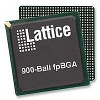
LFE2M70E-5FN900C Lattice, LFE2M70E-5FN900C Datasheet - Page 33

LFE2M70E-5FN900C
Manufacturer Part Number
LFE2M70E-5FN900C
Description
IC, LATTICEECP2M FPGA, 420MHZ, FPBGA-900
Manufacturer
Lattice
Series
LatticeECP2Mr
Datasheet
1.LFE2-12E-5FN256C.pdf
(385 pages)
Specifications of LFE2M70E-5FN900C
No. Of Logic Blocks
67000
No. Of Macrocells
34000
No. Of Speed Grades
5
Total Ram Bits
4534Kbit
No. Of I/o's
416
Clock Management
DLL, PLL
I/o Supply Voltage
3.465V
Rohs Compliant
Yes
Lead Free Status / Rohs Status
Lead free / RoHS Compliant
Available stocks
Company
Part Number
Manufacturer
Quantity
Price
Company:
Part Number:
LFE2M70E-5FN900C
Manufacturer:
Lattice Semiconductor Corporation
Quantity:
10 000
- Current page: 33 of 385
- Download datasheet (3Mb)
Lattice Semiconductor
Table 2-12. PIO Signal List
PIO
The PIO contains four blocks: an input register block, output register block, tristate register block and a control logic
block. These blocks contain registers for operating in a variety of modes along with the necessary clock and selec-
tion logic.
Input Register Block
The input register blocks for PIOs in left, right and bottom edges contain delay elements and registers that can be
used to condition high-speed interface signals, such as DDR memory interfaces and source synchronous inter-
faces, before they are passed to the device core. Figure 2-29 shows the diagram of the input register block for left,
right and bottom edges. The input register block for the top edge contains one memory element to register the input
signal as shown in Figure 2-30. The following description applies to the input register block for PIOs in the left, right
and bottom edges of the device.
Input signals are fed from the sysI/O buffer to the input register block (as signal DI). If desired, the input signal can
bypass the register and delay elements and be used directly as a combinatorial signal (INDD), a clock (INCK) and,
in selected blocks, the input to the DQS delay block. If an input delay is desired, designers can select either a fixed
delay or a dynamic delay DEL[3:0]. The delay, if selected, reduces input register hold time requirements when
using a global clock.
The input block allows three modes of operation. In the single data rate (SDR) the data is registered, by one of the
registers in the single data rate sync register block, with the system clock. In DDR Mode, two registers are used to
sample the data on the positive and negative edges of the DQS signal, creating two data streams, D0 and D1.
These two data streams are synchronized with the system clock before entering the core. Further discussion on
this topic is in the DDR Memory section of this data sheet.
CE0, CE1
CLK0, CLK1
ECLK1, ECLK2
LSR
GSRN
INCK
DQS
INDD
INFF
IPOS0, IPOS1
QPOS0
QNEG0
OPOS0, ONEG0,
OPOS2, ONEG2
OPOS1 ONEG1
DEL[3:0]
TD
DDRCLKPOL
DQSXFER
1. Signals available on left/right/bottom only.
2. Selected I/O.
2
Name
1
1
, QPOS1
, QNEG1
1
1
Control from the core
Control from the core
Control from the core
Control from the core
Control from routing
Input to the core
Input to PIO
Input to the core
Input to the core
Input to the core
Input to the core
Input to the core
Output data from the core
Tristate control from the core
Control from the core
Tristate control from the core
Control from clock polarity bus Controls the polarity of the clock (CLK0) that feed the DDR input block
Control from core
Type
Clock enables for input and output block flip-flops
System clocks for input and output blocks
Fast edge clocks
Local Set/Reset
Global Set/Reset (active low)
Input to Primary Clock Network or PLL reference inputs
DQS signal from logic (routing) to PIO
Unregistered data input to core
Registered input on positive edge of the clock (CLK0)
Double data rate registered inputs to the core
Gearbox pipelined inputs to the core
Gearbox pipelined inputs to the core
Output signals from the core for SDR and DDR operation
Signals to Tristate Register block for DDR operation
Dynamic input delay control bits
Tristate signal from the core used in SDR operation
Controls signal to the Output block
2-30
LatticeECP2/M Family Data Sheet
Description
Architecture
Related parts for LFE2M70E-5FN900C
Image
Part Number
Description
Manufacturer
Datasheet
Request
R
Part Number:
Description:
Manufacturer:
Lattice Semiconductor Corp.
Datasheet:
Part Number:
Description:
IC, LATTICEECP2M FPGA, 420MHZ, FPBGA-900
Manufacturer:
LATTICE SEMICONDUCTOR
Datasheet:

Part Number:
Description:
IC FPGA 50KLUTS 410I/O 900-BGA
Manufacturer:
Lattice
Datasheet:

Part Number:
Description:
IC FPGA 50KLUTS 410I/O 900-BGA
Manufacturer:
Lattice
Datasheet:

Part Number:
Description:
IC FPGA 67KLUTS 1152FPBGA
Manufacturer:
Lattice
Datasheet:

Part Number:
Description:
IC FPGA 67KLUTS 900FPBGA
Manufacturer:
Lattice
Datasheet:

Part Number:
Description:
IC FPGA 67KLUTS 1152FPBGA
Manufacturer:
Lattice
Datasheet:

Part Number:
Description:
IC FPGA 67KLUTS 1152FPBGA
Manufacturer:
Lattice
Datasheet:

Part Number:
Description:
IC FPGA 67KLUTS 1152FPBGA
Manufacturer:
Lattice
Datasheet:

Part Number:
Description:
FPGA - Field Programmable Gate Array 67K LUTs 430 I/O Memry DSP 1.2V -5Spd
Manufacturer:
Lattice

Part Number:
Description:
FPGA - Field Programmable Gate Array 67K LUTs 430 I/O Memry DSP 1.2V -7Spd
Manufacturer:
Lattice

Part Number:
Description:
FPGA - Field Programmable Gate Array 67K LUTs 430 I/O Memry DSP 1.2V -5Spd
Manufacturer:
Lattice

Part Number:
Description:
FPGA - Field Programmable Gate Array 67K LUTs 430 I/O Memry DSP 1.2V -6Spd
Manufacturer:
Lattice

Part Number:
Description:
FPGA - Field Programmable Gate Array 67K LUTs 416 I/O Memory DSP 1.2V 5SPD
Manufacturer:
Lattice


