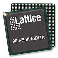
LFE2M70E-5FN900C Lattice, LFE2M70E-5FN900C Datasheet - Page 53

LFE2M70E-5FN900C
Manufacturer Part Number
LFE2M70E-5FN900C
Description
IC, LATTICEECP2M FPGA, 420MHZ, FPBGA-900
Manufacturer
Lattice
Series
LatticeECP2Mr
Datasheet
1.LFE2-12E-5FN256C.pdf
(385 pages)
Specifications of LFE2M70E-5FN900C
No. Of Logic Blocks
67000
No. Of Macrocells
34000
No. Of Speed Grades
5
Total Ram Bits
4534Kbit
No. Of I/o's
416
Clock Management
DLL, PLL
I/o Supply Voltage
3.465V
Rohs Compliant
Yes
Lead Free Status / Rohs Status
Lead free / RoHS Compliant
Available stocks
Company
Part Number
Manufacturer
Quantity
Price
Company:
Part Number:
LFE2M70E-5FN900C
Manufacturer:
Lattice Semiconductor Corporation
Quantity:
10 000
- Current page: 53 of 385
- Download datasheet (3Mb)
Hot Socketing Specifications
Lattice Semiconductor
I
I
1. V
2. 0 ≤ V
3. I
4. LVCMOS and LVTTL only.
5. Assumes that the device is powered down with all supplies grounded, both P and N inputs driven by a CML driver with maximum allowed
DK
HDIN
Symbol
ECP2-12 and ECP2-20 only).
V
DK
CC
CCIB
5
is additive to I
, V
CC
of 1.575V, 8b10b data and internal AC coupling.
CCAUX
≤ V
CC
Input or I/O leakage current
SERDES average input current when
device is powered down and inputs
are driven
and V
(MAX), 0 ≤ V
PU
CCIO
, I
PW
should rise/fall monotonically. V
or I
CCIO
Parameter
BH
.
≤ V
CCIO
(MAX) or 0 ≤ V
1, 2, 3, 4
CC
0 ≤ V
CCAUX
and V
IN
≤ V
≤ V
CCPLL
3-2
CCAUX
Condition
IH
(MAX.)
must be connected to the same power supply (applies to ECP2-6,
(MAX).
DC and Switching Characteristics
LatticeECP2/M Family Data Sheet
Min.
—
—
Typ.
—
—
+/-1000
Max.
4
Units
mA
µA
Related parts for LFE2M70E-5FN900C
Image
Part Number
Description
Manufacturer
Datasheet
Request
R
Part Number:
Description:
Manufacturer:
Lattice Semiconductor Corp.
Datasheet:
Part Number:
Description:
IC, LATTICEECP2M FPGA, 420MHZ, FPBGA-900
Manufacturer:
LATTICE SEMICONDUCTOR
Datasheet:

Part Number:
Description:
IC FPGA 50KLUTS 410I/O 900-BGA
Manufacturer:
Lattice
Datasheet:

Part Number:
Description:
IC FPGA 50KLUTS 410I/O 900-BGA
Manufacturer:
Lattice
Datasheet:

Part Number:
Description:
IC FPGA 67KLUTS 1152FPBGA
Manufacturer:
Lattice
Datasheet:

Part Number:
Description:
IC FPGA 67KLUTS 900FPBGA
Manufacturer:
Lattice
Datasheet:

Part Number:
Description:
IC FPGA 67KLUTS 1152FPBGA
Manufacturer:
Lattice
Datasheet:

Part Number:
Description:
IC FPGA 67KLUTS 1152FPBGA
Manufacturer:
Lattice
Datasheet:

Part Number:
Description:
IC FPGA 67KLUTS 1152FPBGA
Manufacturer:
Lattice
Datasheet:

Part Number:
Description:
FPGA - Field Programmable Gate Array 67K LUTs 430 I/O Memry DSP 1.2V -5Spd
Manufacturer:
Lattice

Part Number:
Description:
FPGA - Field Programmable Gate Array 67K LUTs 430 I/O Memry DSP 1.2V -7Spd
Manufacturer:
Lattice

Part Number:
Description:
FPGA - Field Programmable Gate Array 67K LUTs 430 I/O Memry DSP 1.2V -5Spd
Manufacturer:
Lattice

Part Number:
Description:
FPGA - Field Programmable Gate Array 67K LUTs 430 I/O Memry DSP 1.2V -6Spd
Manufacturer:
Lattice

Part Number:
Description:
FPGA - Field Programmable Gate Array 67K LUTs 416 I/O Memory DSP 1.2V 5SPD
Manufacturer:
Lattice


