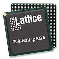
LFE2M70E-5FN900C Lattice, LFE2M70E-5FN900C Datasheet - Page 2

LFE2M70E-5FN900C
Manufacturer Part Number
LFE2M70E-5FN900C
Description
IC, LATTICEECP2M FPGA, 420MHZ, FPBGA-900
Manufacturer
Lattice
Series
LatticeECP2Mr
Datasheet
1.LFE2-12E-5FN256C.pdf
(385 pages)
Specifications of LFE2M70E-5FN900C
No. Of Logic Blocks
67000
No. Of Macrocells
34000
No. Of Speed Grades
5
Total Ram Bits
4534Kbit
No. Of I/o's
416
Clock Management
DLL, PLL
I/o Supply Voltage
3.465V
Rohs Compliant
Yes
Lead Free Status / Rohs Status
Lead free / RoHS Compliant
Available stocks
Company
Part Number
Manufacturer
Quantity
Price
Company:
Part Number:
LFE2M70E-5FN900C
Manufacturer:
Lattice Semiconductor Corporation
Quantity:
10 000
- Current page: 2 of 385
- Download datasheet (3Mb)
June 2008
Features
■ High Logic Density for System Integration
■ Embedded SERDES (LatticeECP2M Only)
■ sysDSP™ Block
■ Flexible Memory Resources
■ sysCLOCK Analog PLLs and DLLs
Table 1-1. LatticeECP2 (Including “S-Series”) Family Selection Guide
© 2007 Lattice Semiconductor Corp. All Lattice trademarks, registered trademarks, patents, and disclaimers are as listed at www.latticesemi.com/legal. All other brand
or product names are trademarks or registered trademarks of their respective holders. The specifications and information herein are subject to change without notice.
www.latticesemi.com
LUTs (K)
Distributed RAM (Kbits)
EBR SRAM (Kbits)
EBR SRAM Blocks
sysDSP Blocks
18x18 Multipliers
GPLL + SPLL + DLL
Maximum Available I/O
Packages and I/O Combinations
144-pin TQFP (20 x 20 mm)
208-pin PQFP (28 x 28 mm)
256-ball fpBGA (17 x 17 mm)
484-ball fpBGA (23 x 23 mm)
672-ball fpBGA (27 x 27 mm)
900-ball fpBGA (31 x 31 mm)
• 6K to 95K LUTs
• 90 to 583 I/Os
• Data Rates 250 Mbps to 3.125 Gbps
• Up to 16 channels per device
• 3 to 42 blocks for high performance multiply and
• Each block supports
• 55Kbits to 5308Kbits sysMEM™ Embedded
• 12K to 202Kbits distributed RAM
• Two GPLLs and up to six SPLLs per device
• Two general purpose DLLs per device
PCI Express, Ethernet (1GbE, SGMII), OBSAI,
CPRI and Serial RapidIO.
accumulate
Block RAM (EBR)
– One 36x36, four 18X18 or eight 9X9 multipliers
– 18Kbit block
– Single, pseudo dual and true dual port
– Byte Enable Mode support
– Single port and pseudo dual port
– Clock multiply, divide, phase & delay adjust
– Dynamic PLL adjustment
Device
ECP2-6
2+0+2
190
190
12
55
12
90
6
3
3
LatticeECP2/M Family Data Sheet
ECP2-12
2+0+2
221
297
131
193
297
12
24
12
24
93
6
1-1
■ Pre-Engineered Source Synchronous I/O
■ Programmable sysI/O™ Buffer Supports
■ Flexible Device Configuration
■ Optional Bitstream Encryption
■ System Level Support
ECP2-20
2+0+2
Wide Range Of Interfaces
(LatticeECP2/M “S” Versions Only)
276
402
131
193
331
402
21
42
15
28
• DDR registers in I/O cells
• Dedicated gearing logic
• Source synchronous standards support
• Dedicated DDR and DDR2 memory support
• Dedicated DQS support
• LVTTL and LVCMOS 33/25/18/15/12
• SSTL 3/2/18 I, II
• HSTL15 I and HSTL18 I, II
• PCI and Differential HSTL, SSTL
• LVDS, RSDS, Bus-LVDS, MLVDS, LVPECL
• 1149.1 Boundary Scan compliant
• Dedicated bank for configuration I/Os
• SPI boot flash interface
• Dual boot images supported
• TransFR™ I/O for simple field updates
• Soft Error Detect macro embedded
• ispTRACY™ internal logic analyzer capability
• On-chip oscillator for initialization & general use
• 1.2V power supply
7
– SPI4.2, SFI4 (DDR Mode), XGMII
– High Speed ADC/DAC devices
– DDR1: 400 (200MHz) / DDR2: 533 (266MHz)
ECP2-35
2+0+2
332
450
331
450
32
64
18
32
8
Introduction
ECP2-50
DS1006
2+2+2
387
500
339
500
48
96
21
18
72
Data Sheet DS1006
Introduction_01.7
ECP2-70
2+4+2
1032
136
583
500
583
68
60
22
88
Related parts for LFE2M70E-5FN900C
Image
Part Number
Description
Manufacturer
Datasheet
Request
R
Part Number:
Description:
Manufacturer:
Lattice Semiconductor Corp.
Datasheet:
Part Number:
Description:
IC, LATTICEECP2M FPGA, 420MHZ, FPBGA-900
Manufacturer:
LATTICE SEMICONDUCTOR
Datasheet:

Part Number:
Description:
IC FPGA 50KLUTS 410I/O 900-BGA
Manufacturer:
Lattice
Datasheet:

Part Number:
Description:
IC FPGA 50KLUTS 410I/O 900-BGA
Manufacturer:
Lattice
Datasheet:

Part Number:
Description:
IC FPGA 67KLUTS 1152FPBGA
Manufacturer:
Lattice
Datasheet:

Part Number:
Description:
IC FPGA 67KLUTS 900FPBGA
Manufacturer:
Lattice
Datasheet:

Part Number:
Description:
IC FPGA 67KLUTS 1152FPBGA
Manufacturer:
Lattice
Datasheet:

Part Number:
Description:
IC FPGA 67KLUTS 1152FPBGA
Manufacturer:
Lattice
Datasheet:

Part Number:
Description:
IC FPGA 67KLUTS 1152FPBGA
Manufacturer:
Lattice
Datasheet:

Part Number:
Description:
FPGA - Field Programmable Gate Array 67K LUTs 430 I/O Memry DSP 1.2V -5Spd
Manufacturer:
Lattice

Part Number:
Description:
FPGA - Field Programmable Gate Array 67K LUTs 430 I/O Memry DSP 1.2V -7Spd
Manufacturer:
Lattice

Part Number:
Description:
FPGA - Field Programmable Gate Array 67K LUTs 430 I/O Memry DSP 1.2V -5Spd
Manufacturer:
Lattice

Part Number:
Description:
FPGA - Field Programmable Gate Array 67K LUTs 430 I/O Memry DSP 1.2V -6Spd
Manufacturer:
Lattice

Part Number:
Description:
FPGA - Field Programmable Gate Array 67K LUTs 416 I/O Memory DSP 1.2V 5SPD
Manufacturer:
Lattice


