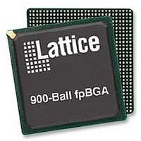
LFE2M70E-5FN900C Lattice, LFE2M70E-5FN900C Datasheet - Page 87

LFE2M70E-5FN900C
Manufacturer Part Number
LFE2M70E-5FN900C
Description
IC, LATTICEECP2M FPGA, 420MHZ, FPBGA-900
Manufacturer
Lattice
Series
LatticeECP2Mr
Datasheet
1.LFE2-12E-5FN256C.pdf
(385 pages)
Specifications of LFE2M70E-5FN900C
No. Of Logic Blocks
67000
No. Of Macrocells
34000
No. Of Speed Grades
5
Total Ram Bits
4534Kbit
No. Of I/o's
416
Clock Management
DLL, PLL
I/o Supply Voltage
3.465V
Rohs Compliant
Yes
Lead Free Status / Rohs Status
Lead free / RoHS Compliant
Available stocks
Company
Part Number
Manufacturer
Quantity
Price
Company:
Part Number:
LFE2M70E-5FN900C
Manufacturer:
Lattice Semiconductor Corporation
Quantity:
10 000
- Current page: 87 of 385
- Download datasheet (3Mb)
Lattice Semiconductor
sysCLOCK SPLL Timing
f
f
f
f
f
AC Characteristics
t
t
t
t
t
t
t
t
t
t
t
1. Jitter sample is taken over 10,000 samples of the primary PLL output with clean reference clock and no additional I/O pins toggling.
2. Output clock is valid after t
3. Using LVDS output buffers.
4. Phase accuracy of CLKOS compared to CLKOP.
5. Value of external capacitor: 5.6 nF ±20%, NPO dielectric, ceramic chip capacitor, 1206 or smaller package, connected to PLLCAP pin.
6. f
Timing v.A 0.11
Parameter
IN
OUT
OUT2
VCO
PFD
DT
PH
OPJIT
SK
W
LOCK
IPJIT
FBKDLY
HI
LO
RST
4
OUT
2
1
(max) = f
Input Clock Frequency (CLKI, CLKFB)
Output Clock Frequency (CLKOP, CLKOS)
K-Divider Output Frequency (CLKOK)
PLL VCO Frequency
Phase Detector Input Frequency
Output Clock Duty Cycle
Output Phase Accuracy
Output Clock Period Jitter
Input Clock to Output Clock Skew
Output Clock Pulse Width
PLL Lock-in Time
Input Clock Period Jitter
External Feedback Delay
Input Clock High Time
Input Clock Low Time
RST Pulse Width (RESETM/RESETK)
Reset Signal Pulse Width (CNTRST)
IN
* 10 for f
IN
LOCK
< 5MHz.
Description
for PLL reset and dynamic delay adjustment.
Over Recommended Operating Conditions
Without external capacitor
With external capacitor
Without external capacitor
With external capacitor
Without external capacitor
With external capacitor
Without external capacitor
With external capacitor
Default Duty Cycle Selected
f
50 ≤ f
f
Divider Ratio = Integer
At 90% or 10%
Without external capacitor
With external capacitor
90% to 90%
10% to 10%
Without external capacitor
With external capacitor
OUT
OUT
3-36
≥ 100 MHz
< 50 MHz
OUT
< 100 MHz
Conditions
DC and Switching Characteristics
LatticeECP2/M Family Data Sheet
5, 6
5
5
6
5
5
3
0.258
0.039
Min.
640
500
0.5
0.5
33
33
33
45
15
20
—
—
—
—
—
—
—
—
—
2
5
2
1
Typ.
50
—
—
—
—
—
—
—
—
—
—
—
—
—
—
—
—
—
—
—
—
—
—
—
—
±0.05
0.025
Max.
1280
±125
±250
±200
0.04
420
420
420
210
420
150
500
50
25
50
55
—
10
—
—
—
—
—
Units
UIPP
UIPP
MHz
MHz
MHz
MHz
MHz
MHz
MHz
MHz
MHz
ns
µs
µs
ns
ns
ns
ns
ns
µs
%
UI
ps
ps
ps
Related parts for LFE2M70E-5FN900C
Image
Part Number
Description
Manufacturer
Datasheet
Request
R
Part Number:
Description:
Manufacturer:
Lattice Semiconductor Corp.
Datasheet:
Part Number:
Description:
IC, LATTICEECP2M FPGA, 420MHZ, FPBGA-900
Manufacturer:
LATTICE SEMICONDUCTOR
Datasheet:

Part Number:
Description:
IC FPGA 50KLUTS 410I/O 900-BGA
Manufacturer:
Lattice
Datasheet:

Part Number:
Description:
IC FPGA 50KLUTS 410I/O 900-BGA
Manufacturer:
Lattice
Datasheet:

Part Number:
Description:
IC FPGA 67KLUTS 1152FPBGA
Manufacturer:
Lattice
Datasheet:

Part Number:
Description:
IC FPGA 67KLUTS 900FPBGA
Manufacturer:
Lattice
Datasheet:

Part Number:
Description:
IC FPGA 67KLUTS 1152FPBGA
Manufacturer:
Lattice
Datasheet:

Part Number:
Description:
IC FPGA 67KLUTS 1152FPBGA
Manufacturer:
Lattice
Datasheet:

Part Number:
Description:
IC FPGA 67KLUTS 1152FPBGA
Manufacturer:
Lattice
Datasheet:

Part Number:
Description:
FPGA - Field Programmable Gate Array 67K LUTs 430 I/O Memry DSP 1.2V -5Spd
Manufacturer:
Lattice

Part Number:
Description:
FPGA - Field Programmable Gate Array 67K LUTs 430 I/O Memry DSP 1.2V -7Spd
Manufacturer:
Lattice

Part Number:
Description:
FPGA - Field Programmable Gate Array 67K LUTs 430 I/O Memry DSP 1.2V -5Spd
Manufacturer:
Lattice

Part Number:
Description:
FPGA - Field Programmable Gate Array 67K LUTs 430 I/O Memry DSP 1.2V -6Spd
Manufacturer:
Lattice

Part Number:
Description:
FPGA - Field Programmable Gate Array 67K LUTs 416 I/O Memory DSP 1.2V 5SPD
Manufacturer:
Lattice


