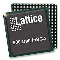
LFE2M70E-5FN900C Lattice, LFE2M70E-5FN900C Datasheet - Page 384

LFE2M70E-5FN900C
Manufacturer Part Number
LFE2M70E-5FN900C
Description
IC, LATTICEECP2M FPGA, 420MHZ, FPBGA-900
Manufacturer
Lattice
Series
LatticeECP2Mr
Datasheet
1.LFE2-12E-5FN256C.pdf
(385 pages)
Specifications of LFE2M70E-5FN900C
No. Of Logic Blocks
67000
No. Of Macrocells
34000
No. Of Speed Grades
5
Total Ram Bits
4534Kbit
No. Of I/o's
416
Clock Management
DLL, PLL
I/o Supply Voltage
3.465V
Rohs Compliant
Yes
Lead Free Status / Rohs Status
Lead free / RoHS Compliant
Available stocks
Company
Part Number
Manufacturer
Quantity
Price
Company:
Part Number:
LFE2M70E-5FN900C
Manufacturer:
Lattice Semiconductor Corporation
Quantity:
10 000
- Current page: 384 of 385
- Download datasheet (3Mb)
Lattice Semiconductor
September 2006
September 2006
December 2006
February 2007
August 2007
August 2006
March 2007
March 2007
April 2007
July 2007
(cont.)
Date
Version
(cont.)
02.0
02.1
02.2
02.3
02.4
02.5
02.6
02.7
02.8
01.1
Ordering Information
Ordering Information
Ordering Information
Ordering Information Updated ordering part number table to include ECP2-12.
Pinout Information
Pinout Information
DC and Switching
DC and Switching
DC and Switching
DC and Switching
DC and Switching
DC and Switching
Pinout Information
Characteristics
Characteristics
Architecture
Architecture
Architecture
Architecture
Architecture
Introduction
Introduction
Introduction
Introduction
Section
Multiple
(cont.)
Added Information on: Available Device Resources per Packaged
Device table
Updated topside mark drawing
Added information regarding LatticeECP2M support throughout.
Added Receiver Total Jitter Tolerance Specification table.
Removed power-up requirements for proper configuration footnote in
Recommended Operating Conditions table.
LatticeECP2M Selection Guide table has been updated.
Figure 2-16. Per Region Secondary Clock Selection has been updated.
Figure 2-39. Simplified Channel Block Diagram for SERDES and PCS
has been updated.
Footnotes have been added to Recommended Operating Conditions
DC Electrical Characteristics table has been updated.
Supply Current (Standby) tables have been updated.
Initialization Supply Current table have been updated.
Updated timing numbers to include LFE2-12E (rev A 0.08)
Updated to include the entire ECP2 device information as well as 256-
fpBGA and 484-fpBGA pin information for the ECP2M35E.
Updated to include the entire ECP2 and ECP2M device ordering infor-
mation.
Updated EBR Asynchronous Reset section.
Power-sequencing footnotes have been added to the Recommended
Operating Conditions. DDR2 performance has been updated to
266MHz.
Added “Security Series” to the LatticeECP2 and LatticeECP2M
families.
Enhanced Configuration Option section updated.
Recommended Operating Conditions table - footnote 4 updated.
“Security Series” ordering part numbers added.
LatticeECP2M family table has been updated for user I/O counts.
LatticeECP2M family ordering part number section has been updated to
add 1152-fpBGA package for the ECP2M70 and ECP2M100.
Updated text in Ripple Mode section.
ECP2/M Supply Current information has been updated.
Typical Building Block Function Performance, External Switching Char-
acteristics, Internal Switching Characteristics, Family Timing Adders,
sysCLOCK GPLL Timing, sysCLOCK SPLL Timing, DLL Timing and
sysCONFIG Port Timing Specifications have been updated (timing rev.
A 0.10).
SERDES timing information has been updated.
PCI Express timing information has been updated.
Added LatticeECP2M20 pinout information.
1156-fpBGA package option has been removed from the LatticeECP2M
family.
Table 2-16. Selectable Master Clock (CCLK) Frequencies During Con-
figuration table has been updated.
Supply Current (Standby) table has been updated.
DSP Function timing has been updated.
7-2
LatticeECP2/M Family Data Sheet
Change Summary
Revision History
Related parts for LFE2M70E-5FN900C
Image
Part Number
Description
Manufacturer
Datasheet
Request
R
Part Number:
Description:
Manufacturer:
Lattice Semiconductor Corp.
Datasheet:
Part Number:
Description:
IC, LATTICEECP2M FPGA, 420MHZ, FPBGA-900
Manufacturer:
LATTICE SEMICONDUCTOR
Datasheet:

Part Number:
Description:
IC FPGA 50KLUTS 410I/O 900-BGA
Manufacturer:
Lattice
Datasheet:

Part Number:
Description:
IC FPGA 50KLUTS 410I/O 900-BGA
Manufacturer:
Lattice
Datasheet:

Part Number:
Description:
IC FPGA 67KLUTS 1152FPBGA
Manufacturer:
Lattice
Datasheet:

Part Number:
Description:
IC FPGA 67KLUTS 900FPBGA
Manufacturer:
Lattice
Datasheet:

Part Number:
Description:
IC FPGA 67KLUTS 1152FPBGA
Manufacturer:
Lattice
Datasheet:

Part Number:
Description:
IC FPGA 67KLUTS 1152FPBGA
Manufacturer:
Lattice
Datasheet:

Part Number:
Description:
IC FPGA 67KLUTS 1152FPBGA
Manufacturer:
Lattice
Datasheet:

Part Number:
Description:
FPGA - Field Programmable Gate Array 67K LUTs 430 I/O Memry DSP 1.2V -5Spd
Manufacturer:
Lattice

Part Number:
Description:
FPGA - Field Programmable Gate Array 67K LUTs 430 I/O Memry DSP 1.2V -7Spd
Manufacturer:
Lattice

Part Number:
Description:
FPGA - Field Programmable Gate Array 67K LUTs 430 I/O Memry DSP 1.2V -5Spd
Manufacturer:
Lattice

Part Number:
Description:
FPGA - Field Programmable Gate Array 67K LUTs 430 I/O Memry DSP 1.2V -6Spd
Manufacturer:
Lattice

Part Number:
Description:
FPGA - Field Programmable Gate Array 67K LUTs 416 I/O Memory DSP 1.2V 5SPD
Manufacturer:
Lattice


