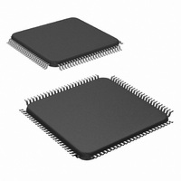
DS90C387RVJDX/NOPB National Semiconductor, DS90C387RVJDX/NOPB Datasheet - Page 11

DS90C387RVJDX/NOPB
Manufacturer Part Number
DS90C387RVJDX/NOPB
Description
IC LDI DUAL PIXAL 3.3V 100-TQFP
Manufacturer
National Semiconductor
Datasheet
1.DS90C387RVJDXNOPB.pdf
(28 pages)
Specifications of DS90C387RVJDX/NOPB
Applications
Displays
Interface
2-Wire Serial
Voltage - Supply
3 V ~ 3.6 V
Package / Case
100-TQFP, 100-VQFP
Mounting Type
Surface Mount
Lead Free Status / RoHS Status
Lead free / RoHS Compliant
Other names
DS90C387RVJDX
Available stocks
Company
Part Number
Manufacturer
Quantity
Price
Company:
Part Number:
DS90C387RVJDX/NOPB
Manufacturer:
Texas Instruments
Quantity:
10 000
DS90C387R Pin Description—LDI
Transmitter
D0-D23
DE
HSYNC
VSYNC
AnP
AnM
CLKINP
CLKINM
R_FB
R_FDE
CLK1P
CLK1M
PD
PLLSEL
BAL
PRE
DUAL
V
GND
I2V
V
GND
SGND
CC
CC3V
Pin Name
CC
3V
I/O
O
O
O
O
I
I
I
I
I
I
I
I
I
I
I
I
I
I
I
I
I
I
I
No.
24
1
1
1
8
8
1
1
1
1
1
1
1
1
1
1
1
1
4
1
3
3
1
LVTTL level single-ended inputs or low swing pseduo differential inputs.
Reference to V
D0-D11 are for 12-bit input mode (24 RGB data); D0-D11 (first 12-bit port)
and D12-D23 (second 12-bit port) are for two 12-bit input mode (48 RGB
data).
LVTTL level or low swing level inputs for data enable. This signal is HIGH
when input pixel data is valid to DS90C387R provided that R_FDE = HIGH.
Horizontal Sync input control signal. LVTTL level or low swing level.
Vertical Horizontal Sync input control signal. LVTTL level or low swing level.
Positive LVDS differential data output.
Negative LVDS differential data output.
In LVTTL level operation, this is a single-ended clock. In low swing
operation, this is the positive differential clock input .
In LVTTL level operation, no connect or connect to V
to GND under any condition. In low swing operation, this is negative
differential clock input .
LVTTL level input for selecting the Primary clock edge E1. Falling clock
edge selected when input is HIGH; Rising clock edge selected when input is
LOW.(Note 14)
LVTTL level input. Programmable control (DE) strobe select. Tie HIGH for
data active when DE is HIGH. (Note 14)
Positive LVDS differential clock output.
Negative LVDS differential clock output.
LVCMOS level input. Input = LOW will place the entire device in power down
mode. Outputs of the device will be in TRI-STATE mode to ensure low
current at power down. (Note 14)
Input = HIGH for normal operation.
LVTTL level in. Tie to Vcc for normal operation. (Note 14)
LVTTL level input. Mode select for dc balanced or non-dc balanced
interface. DC balance is active when input is high. (Note 14)
Pre-emphasis level select. Pre-emphasis is active when input is tied to V
through external pull-up resistor. Resistor value determines pre-emphasis
level (see table in application section). For normal LVDS drive level
(minimum pre-emphasis) leave this pin open (do not tie to ground).(Note 14)
LVTTL level input. Input = LOW for one 12-bit input mode, 24 RGB data in,
24 RGB data out.(Note 14)
LVTTL level input. Input = V
48 RGB data out.(Note 14)
Connect to power supply with voltage stated under ” Recommended
Operating Conitions ” on page 3. Power supply pin for LVTTL inputs and
digital circuitry, pin53.
Ground pins for LVTTL inputs and digital circuitry, pins 9, 11, 52, 77.
Connect to power supply with voltage stated under ” Recommended
Operating Conitions ” on page 3, pin 68.
Connect to power supply with voltage stated under ” Recommended
Operating Conitions ” on page 3, pins 70, 79, 95.
Ground pin(s) for powering the data inputs, pins 71, 80, 96.
Connect to ground, pin 69.
11
REF
pin.
CC
for two 12-bit input mode, 48 RGB data in,
Description
REF
pin. Do not connect
www.national.com
CC


