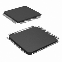
DS90C387RVJDX/NOPB National Semiconductor, DS90C387RVJDX/NOPB Datasheet - Page 15

DS90C387RVJDX/NOPB
Manufacturer Part Number
DS90C387RVJDX/NOPB
Description
IC LDI DUAL PIXAL 3.3V 100-TQFP
Manufacturer
National Semiconductor
Datasheet
1.DS90C387RVJDXNOPB.pdf
(28 pages)
Specifications of DS90C387RVJDX/NOPB
Applications
Displays
Interface
2-Wire Serial
Voltage - Supply
3 V ~ 3.6 V
Package / Case
100-TQFP, 100-VQFP
Mounting Type
Surface Mount
Lead Free Status / RoHS Status
Lead free / RoHS Compliant
Other names
DS90C387RVJDX
Available stocks
Company
Part Number
Manufacturer
Quantity
Price
Company:
Part Number:
DS90C387RVJDX/NOPB
Manufacturer:
Texas Instruments
Quantity:
10 000
Two-Wire Serial Communication Interface Description
FRQ_HIGH
FRQ_LOW
MSEL [2:0]
*CFG [7:0]
DEV_REV
VND_IDH
DEV_IDH
VND_IDL
DEV_IDL
CTL [3:1]
*HTPLG
VLOW
EDGE
RSEN
BSEL
DSEL
TSEL
Field
HEN
VEN
MDI
PD
TABLE 4. Register Field Definitions(’ * " = features not implemented on DS90C387R)
Access
RW
RW
RW
RW
RW
RW
RW
RW
RW
RW
RO
RO
RO
RO
RO
RO
RO
RO
RO
RO
RO
Vendor ID low byte, value is 05h.
Vendor ID high byte, value is 13h.
Device ID low byte, value is 24h.
Device ID high byte, value is 67h.
Device revision, value is 00h.
25 MHz is Low frequency limit for the current mode, value is 19h.
85 MHz is High frequency limit for the current mode, value is 55h.
Power down mode, default = 1.
0 - power down only the LVDS drivers. Output of this device will be in TRI-STATE
mode. Other circuitry are still active.
1 - normal operation.
Edge select (same function as R_FB pin), default = 1.
0 - input data is rising edge latched (rising edge latched first in 12-bit and two 12-bit
mode).
1 - input data is falling edge latched (falling edge latched first in 12-bit and two 12-bit
mode).
Input bus select (same as DUAL pin), default = 0.
0 - one 12-bit bus.
1 - two 12-bit bus.
Dual level clock select (same function as DSEL pin), default = 1.
0 - input clock is differential.
1 - input clock is single-ended (up to 65MHz). CLKINM and V
connected.
Horizontal sync enable, default = 1.
0 - HSYNC input is transmitted as fixed LOW.
1 - HSYNC input is transmitted as it is.
Vertical sync enable, default = 1.
0 - VSYNC input is transmitted as fixed LOW.
1 - VSYNC input is transmitted as it is.
Monitor Detect Interrupt, default = 1.
0 - Detection signal has changed logical level (write "1" to this bit to clear).
1 - Detection signal has not changed state.
Feature not implemented.
This bit is a ”1 “ if a powered on receiver is connected to the transmitter outputs, ” 0 “
otherwsie. This function is only available for use in DC-coupled systems. Default=0.
Interrupt generation method, default=0.
0 - Interrupt bit (MDI) is generated by monitoring RSEN.
1 - Interrupt bit (MDI) is generated by monitoring HTPLG.
Select source for the MSEN output pin. Default valus is 001.
000 - Force MSEN output HIGH (disabled).
001 - Output the value of MDI bit (interrupt). This is default.
010 - Output the value of RSEN bit (receiver detect).
011 - Output the value of HTPLG bit (hot plug detect).
1xx - Reserved.
This bit is an 1 if the VREF signal indicates low swing inputs. Default=1.
It is a 0 if VREF indicates high swing inputs.
General purpose inputs.
Feature not implemented.
15
Description
(Continued)
REF
pin are internally
www.national.com


