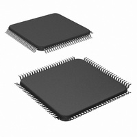
DS90C387RVJDX/NOPB National Semiconductor, DS90C387RVJDX/NOPB Datasheet - Page 14

DS90C387RVJDX/NOPB
Manufacturer Part Number
DS90C387RVJDX/NOPB
Description
IC LDI DUAL PIXAL 3.3V 100-TQFP
Manufacturer
National Semiconductor
Datasheet
1.DS90C387RVJDXNOPB.pdf
(28 pages)
Specifications of DS90C387RVJDX/NOPB
Applications
Displays
Interface
2-Wire Serial
Voltage - Supply
3 V ~ 3.6 V
Package / Case
100-TQFP, 100-VQFP
Mounting Type
Surface Mount
Lead Free Status / RoHS Status
Lead free / RoHS Compliant
Other names
DS90C387RVJDX
Available stocks
Company
Part Number
Manufacturer
Quantity
Price
Company:
Part Number:
DS90C387RVJDX/NOPB
Manufacturer:
Texas Instruments
Quantity:
10 000
www.national.com
DS90C387R Pin Description—LDI Transmitter
Two-Wire Serial Communication Interface Description
The DS90C387R operates as a slave on the Serial Bus, so
the SCL line is an input (no clock is generated by the
DS90C387R) and the SDA line is bi-directional. DS90C387R
has a 7-bit slave address. The address bits are controlled by
the state of the address select pins A2, A1 and A0, and are
set by connecting these pins to ground for a LOW, (0) , to
V
The DS90C387R latches the state of the address select pins
during the first read or write on the Serial Bus. Changing the
state of the address select pins after the first read or write to
any device on the Serial Bus will not change the slave
address of the DS90C387R.
CC
Addr
00C
00D
00A
00B
00E
00F
000
001
002
003
004
005
006
007
008
009
R_FB
VCC
GND
for a HIGH, (1).
VLOW(RO)
Bit7
Primary Edge
RSVD[1:0]
Falling
Rising
TABLE 3. Register Mapping(" * ’ = features not implemented on DS90C387R)
*DK[3:1](RW)
TABLE 2. Relationship between R_FB, DE, HSYNC and VSYNC pins
Bit6
RSVD[3:0](RW)
A2
MSEL[2:0](RW)
0
0
0
0
1
1
1
1
Secondary Edge
Address Select Pin
VEN(RW)
Bit5
Falling
Rising
State
A1
0
0
1
1
0
0
1
1
*DKEN(RW)
HEN(RW)
FRQ_HIGH[7:0](RO)
FRQ_LOW[7:0](RO)
Bit4
*VDJK[7:0](RW)
RSVD[7:0](RW)
RSVD[7:0](RW)
DEV_REV(RO)
RSVD[7:0](RO)
VND_IDH(RO)
*CFG[7:0](RO)
A0
VND_IDL(RO)
DEV_IDH(RO)
DEV_IDL(RO)
0
1
0
1
0
1
0
1
14
DE latches on
Therefore, the complete slave address is:
and is selected as follows:
A zero in front of the register address is required as the most
left column shown in the table below. For example, to access
register F, “0F” is the correct way of accessing the register.
Falling
Rising
DSEL(RW)
MSB
TSEL(RW)
A6
Bus Slave Address
DS90C387R Serial
Bit3
A6:A0 binary
0111000
0111001
0111010
0111011
0111100
0111101
0111110
0111111
A5
(Continued)
CTL[3:1](RW)
HSYNC latches on
RSEN(RO)
BSEL(RW)
A4
Bit2
RSVD[3:0](RO)
Falling
Rising
A3
*HTPLG(RO)
EDGE(RW)
Bit1
A2
VSYNC latches on
Falling
Rising
A1
RSVD(RW)
MDI(RW)
PD(RW)
Bit0
LSB
A0


