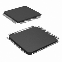
DS90C387RVJDX/NOPB National Semiconductor, DS90C387RVJDX/NOPB Datasheet - Page 26

DS90C387RVJDX/NOPB
Manufacturer Part Number
DS90C387RVJDX/NOPB
Description
IC LDI DUAL PIXAL 3.3V 100-TQFP
Manufacturer
National Semiconductor
Datasheet
1.DS90C387RVJDXNOPB.pdf
(28 pages)
Specifications of DS90C387RVJDX/NOPB
Applications
Displays
Interface
2-Wire Serial
Voltage - Supply
3 V ~ 3.6 V
Package / Case
100-TQFP, 100-VQFP
Mounting Type
Surface Mount
Lead Free Status / RoHS Status
Lead free / RoHS Compliant
Other names
DS90C387RVJDX
Available stocks
Company
Part Number
Manufacturer
Quantity
Price
Company:
Part Number:
DS90C387RVJDX/NOPB
Manufacturer:
Texas Instruments
Quantity:
10 000
www.national.com
Applications Information
feature supports backward compatibility with the previous
generation of devices - the second clock allows the transmit-
ter to interface to panels using a ’dual pixel’ configuration of
two 24-bit or 18-bit ’notebook’ receivers.
Pre-emphasis feature is available for use in both the DC
balanced and non-DC balanced (backwards compatible)
modes.
Information on Jitter Rejection:
The transmitter is designed to reject cycle-to-cycle jitter
which may be seen at the transmitter input clock. Very low
cycle-to-cycle jitter is passed on to the transmitter outputs.
Transmitter Block Diagram
Configuration Table
R_FB (Tx only)
R_FDE (both Tx and Rx)
BAL (both Tx and Rx)
DUAL (Tx only)
Pin
TABLE 12. Transmitter / DS90CF388 Receiver configuration table
R_FB = V
R_FB = GND
R_FDE = V
R_FDE = GND
BAL=V
BAL=Gnd
DUAL=V
DUAL=Gnd
Condition
CC
(Continued)
CC
CC
CC
Primary clock edge selected as Falling Edge
Primary clock edge selected as Rising Edge
Active data DE = High
Active data DE = Low
DC Balanced enabled
DC Balanced disabled (backward compatible to FPD-Link)
48-bit color (dual pixel) support
24-bit color (single pixel) support
26
This significantly reduces the impact of jitter provided by the
input clock source, and improves the accuracy of data sam-
pling. Data sampling is further enhanced by automatically
calibrated data sampling strobes at the receiver inputs. Tim-
ing and control signals (VSYNC, HSYNC, DE) are sent
during blanking intervals to guarantee correct reception of
these critical signals.
The transmitter is offered with programmable primary clock
edge for convenient interface with a variety of graphics
controllers. The transmitter can be programmed for rising
edge strobe or falling edge strobe through a dedicated pin. A
rising edge transmitter will inter-operate with a falling edge
receiver without any translation logic.
Configuration
10128802


