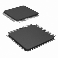
DS90C387RVJDX/NOPB National Semiconductor, DS90C387RVJDX/NOPB Datasheet - Page 6

DS90C387RVJDX/NOPB
Manufacturer Part Number
DS90C387RVJDX/NOPB
Description
IC LDI DUAL PIXAL 3.3V 100-TQFP
Manufacturer
National Semiconductor
Datasheet
1.DS90C387RVJDXNOPB.pdf
(28 pages)
Specifications of DS90C387RVJDX/NOPB
Applications
Displays
Interface
2-Wire Serial
Voltage - Supply
3 V ~ 3.6 V
Package / Case
100-TQFP, 100-VQFP
Mounting Type
Surface Mount
Lead Free Status / RoHS Status
Lead free / RoHS Compliant
Other names
DS90C387RVJDX
Available stocks
Company
Part Number
Manufacturer
Quantity
Price
Company:
Part Number:
DS90C387RVJDX/NOPB
Manufacturer:
Texas Instruments
Quantity:
10 000
www.national.com
t
t
t
t
t
1
2
3
4
5
Symbol
Transmitter Switching Characteristics
Note 5: The limits are based on bench characterization of the device’s jitter response over the power supply voltage range. Output clock jitter is measured with a
cycle-to-cycle jitter of
in the clock edge from most graphics VGA chips currently available. This parameter is used when calculating system margin as described in AN-1059.
Note 6: Receiver Skew Margin is defined as the valid data sampling region at the receiver inputs. This margin takes into account transmitter output pulse positions
(min and max) and the receiver input setup and hold time (internal data sampling window - RSPOS). This margin allows for LVDS interconnect skew, inter-symbol
interference (both dependent on type/length of cable) and clock jitter.
RSKM ≥ cable skew (type, length) + source clock jitter (cycle to cycle).
Note 7: This limit is based on the capability of deskew circuitry. This margin allows for LVDS interconnect skew, inter-symbol interference (both dependent on
type/length of cable) and clock jitter. RSKM with deskew is
Note 8: The parameters are guaranteed by design. The limits are based on statistical analysis of the device performance over PVT(process, voltage and
temperature) range.
Note 9: From V = 1.5V of CLKINP to V
DIGITAL SWITCHING CHARACTERISTICS for Two-Wire Serial
Communication Interface
AC Timing Diagrams
Unless otherwise noted, below specifications apply for V
on output lines can be up to 400 pF provided that external pull-up switch is on board. The following parameters are the timing
relationships between SCL and SDA signals related to the DS90C387R.
SCL (Clock) Period
Data in Set-Up Time to SCL High
Data Out Stable after SCL Low
SDA Low Set-Up Time to SCL Low (Start Condition)
SDA High Hold Time after SCL High (Stop Condition)
FIGURE 1. Two-Wire Serial Communication Interface Timing Diagram when I2CSEL = Vcc
±
2ns applied to the input clock signal while data inputs are switching (see figures 10 and 11). A jitter event of 2ns, represents worse case jump
DIFF
= 0V of CLK1P when R_FB = High, DUAL = Low or High, BAL = Low.
Parameter
±
1 LVDS bit time (1/7th clock period) data to clock skew.
cc
=+3.3V, load capacitance on output lines = 80 pF. Load capacitance
6
(Continued)
Min
100
100
100
2.5
0
Typ
10128832
Max
Units
µs
ns
ns
ns
ns


