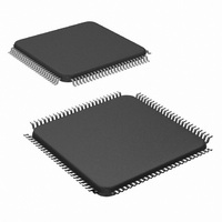
DS90C387RVJDX/NOPB National Semiconductor, DS90C387RVJDX/NOPB Datasheet - Page 5

DS90C387RVJDX/NOPB
Manufacturer Part Number
DS90C387RVJDX/NOPB
Description
IC LDI DUAL PIXAL 3.3V 100-TQFP
Manufacturer
National Semiconductor
Datasheet
1.DS90C387RVJDXNOPB.pdf
(28 pages)
Specifications of DS90C387RVJDX/NOPB
Applications
Displays
Interface
2-Wire Serial
Voltage - Supply
3 V ~ 3.6 V
Package / Case
100-TQFP, 100-VQFP
Mounting Type
Surface Mount
Lead Free Status / RoHS Status
Lead free / RoHS Compliant
Other names
DS90C387RVJDX
Available stocks
Company
Part Number
Manufacturer
Quantity
Price
Company:
Part Number:
DS90C387RVJDX/NOPB
Manufacturer:
Texas Instruments
Quantity:
10 000
LLHT
LHLT
TCCS
TPPOS0
TPPOS1
TPPOS2
TPPOS3
TPPOS4
TPPOS5
TPPOS6
TSTC
THTC
TJCC
TPLLS
TPDD
TPDL
TCIT
TCIP
TCIH
TCIL
VDDQ
Symbol
Symbol
Recommended Transmitter Input Characteristics
Over recommended operating supply and temperature ranges unless otherwise specified. Device driving the transmitter inputs
should comply to this table of recommendations.
Transmitter Switching Characteristics
Over recommended operating supply and temperature ranges unless otherwise specified.(Note 2)
TxCLK IN Transition Time (Figure 5)
TxCLK IN Period (Figure 6)
TxCLK in High Time (Figure 6)
TxCLK in Low Time (Figure 6)
Low Swing Voltage Amplitude from GMCH
LVDS Low-to-High Transition Time (Figure 4), PRE = no connect
(minimum pre-empahsis).
LVDS Low-to-High Transition Time (Figure 4), PRE = V
pre-empahsis).
LVDS High-to-Low Transition Time (Figure 4), PRE = no connect
(mini. pre-empahsis).
LVDS High-to-Low Transition Time (Figure 4), PRE = V
pre-empahsis).
TxOUT Channel to Channel Skew
Transmitter Output Pulse Position for Bit0
from TxCLKout rising edge.
Transmitter Output Pulse Position for Bit1
from TxCLKout rising edge.
Transmitter Output Pulse Position for Bit2
from TxCLKout rising edge.
Transmitter Output Pulse Position for Bit3
from TxCLKout rising edge.
Transmitter Output Pulse Position for Bit4
from TxCLKout rising edge.
Transmitter Output Pulse Position for Bit5
from TxCLKout rising edge.
Transmitter Output Pulse Position for Bit6
from TxCLKout rising edge.
TxIN Setup to TxCLK IN in low swing mode at 85 MHz (Figure 7)
TxIN Hold to TxCLK IN in low swing mode at 85 MHz (Figure 7)
Transmitter Jitter Cycle-to-cycle (Figures
12, 13) (Note 5), DUAL = Gnd, V
Transmitter Phase Lock Loop Set (Figure 8)
Transmitter Powerdown Delay (Figure 9)
Transmitter Input to Output Latency (Figure
10)
Parameter
Parameter
CC
= 3V
f = 85MHz (Note 8)
f = 85 MHz
f = 65 MHz
f = 32.5 MHz
f = 32.5/65/85 MHz
(Note 9)
DUAL = Gnd or V
DUAL = Gnd or V
5
CC
CC
(max.
(max.
CC
CC
-300
1.38
3.06
4.74
6.42
8.10
9.78
11.76
Min
0.4T
0.4T
1.8
Min
0.8
1.0
2
1.5TCIP
10.08
+4.1
0.14
0.11
0.16
0.11
1.68
3.36
5.04
6.72
8.40
Typ
0.5T
0.5T
100
110
Typ
1.2
80
75
0
T
+300
1.98
3.66
5.34
7.02
8.70
10.38
Max
Max
0.6T
0.6T
150
120
115
100
0.9
0.7
0.9
0.7
2.4
1.8
10
40
www.national.com
Units
Units
ms
ns
ns
ns
ns
ns
ns
ns
ns
ps
ps
ns
ns
ns
ns
ns
ns
ns
ns
ps
ps
ps
ns
ns
V


