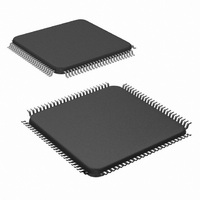
DS90C387RVJDX/NOPB National Semiconductor, DS90C387RVJDX/NOPB Datasheet - Page 12

DS90C387RVJDX/NOPB
Manufacturer Part Number
DS90C387RVJDX/NOPB
Description
IC LDI DUAL PIXAL 3.3V 100-TQFP
Manufacturer
National Semiconductor
Datasheet
1.DS90C387RVJDXNOPB.pdf
(28 pages)
Specifications of DS90C387RVJDX/NOPB
Applications
Displays
Interface
2-Wire Serial
Voltage - Supply
3 V ~ 3.6 V
Package / Case
100-TQFP, 100-VQFP
Mounting Type
Surface Mount
Lead Free Status / RoHS Status
Lead free / RoHS Compliant
Other names
DS90C387RVJDX
Available stocks
Company
Part Number
Manufacturer
Quantity
Price
Company:
Part Number:
DS90C387RVJDX/NOPB
Manufacturer:
Texas Instruments
Quantity:
10 000
www.national.com
DS90C387R Pin Description—LDI Transmitter
Note 14: Inputs default to “low” when left open due to internal pull-down resistor.
PLLV
PLLGND
LVDSV
LVDSGND
CLK2P/NC
CLK2M/NC
V
I2CSEL
DDREN/I2Cclk
DSEL/I2Cdat
A0
A1
A2
MSEN
TST1
TST2
RESERVED1
RESERVED2
RESERVED3
RESERVED4
RESERVED5
RESERVED6
RESERVED7
RESERVED8
RESERVED9
REF
Pin Name
CC
CC
I
I/O
I/O
O
O
O
I
I
I
I
I
I
I
I
I
DDREN/I2Cclk
CLKIN polarity
I2CSEL
Mode
DUAL
BAL
No.
2
3
3
4
1
1
1
1
1
1
1
1
1
1
1
1
1
1
1
1
1
1
1
1
1
TABLE 1. Control Settings for mode selection
Connect to power supply with voltage stated under ” Recommended
Operating Conitions ” on page 3. Power supply pins for PLL circuitry, pin 10,
16.
Ground pins for PLL circuitry, pins 14, 15, 17.
Connect to power supply with voltage stated under ” Recommended
Operating Conitions ” on page 3. Power supply pins for LVDS outputs, pins
30, 40, 48.
Ground pins for LVDS outputs, pins 25, 35, 43, 51.
Additional positive LVDS differential clock output identical to CLK1P. No
connect if not used.
Additional negative LVDS differential clock output identical to CLK1M. No
connect if not used.
V
If V
If V
In low voltage swing mode, input data = logic HIGH = V
In low voltage swing mode, input data = logic LOW = V
This pin is not to be left floating. When not use in LVTTL mode, tie to V
HIGH to enable two-wire serial communication interface; LOW to disable the
interface.
Always HIGH for one 12-bit port and two 12-bit ports operation. When
I2CSEL = HIGH, this is the clock line for the two-wire serial communication
interface.
Differential select pin for CLKIN (HIGH = single-ended, LOW = differentail)
or when I2CSEL = HIGH, this is the Bidirectional Data line for the two-wire
serial communication interface.
when I2CSEL = HIGH, this is one of the Slave Device Address Lower Bits.
when I2CSEL = HIGH, this is one of the Slave Device Address Lower Bits.
when I2CSEL = HIGH, this is one of the Slave Device Address Lower Bits.
Interrupt signal. This is an open drain output, pull-up resistor is required.
Test pin, tie to Vcc.
Test pin, no connect. Do not tie to ground.
Reserved pin, tie to ground.
Reserved pin, tie to ground.
Reserved pin, no connect. Do not tie to ground.
Reserved pin, tie to ground.
Reserved pin, tie to ground.
Reserved pin, tie to ground.
Reserved pin, tie to ground.
Reserved pin, tie to ground.
Reserved pin, tie to ground.
REF
REF
REF
= 1/2 V
≥ 1.8V, indicates input data is in LVTTL mode.
<
1.1V, indicates input data is in low voltage swing mode.
R_FB
12bit
DDQ
L/H
12
H
L
L
, a ”Fixed “ line of differential input.
(Continued)
Description
Two 12-bit
R_FB
L/H
H
H
L
REF
REF
- 100mV.
+ 100mV.
cc


