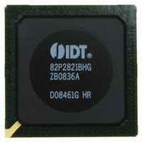
IDT82P2821BHG IDT, Integrated Device Technology Inc, IDT82P2821BHG Datasheet - Page 10

IDT82P2821BHG
Manufacturer Part Number
IDT82P2821BHG
Description
IC LINE INTERFACE UNIT 640-PBGA
Manufacturer
IDT, Integrated Device Technology Inc
Datasheet
1.IDT82P2821BHG.pdf
(151 pages)
Specifications of IDT82P2821BHG
Function
Line Interface Unit (LIU)
Interface
E1, J1, T1
Number Of Circuits
1
Voltage - Supply
1.8V, 3.3V
Operating Temperature
-40°C ~ 85°C
Mounting Type
Surface Mount
Package / Case
*
Includes
Defect and Alarm Detection, Driver Over-Current Detection and Protection, LLOS Detection, PRBSARB / IB Detection and Generation
Number Of Transceivers
1
Screening Level
Industrial
Mounting
Surface Mount
Operating Temperature (min)
-40C
Operating Temperature (max)
85C
Lead Free Status / RoHS Status
Lead free / RoHS Compliant
Current - Supply
-
Power (watts)
-
Lead Free Status / RoHS Status
Compliant, Lead free / RoHS Compliant
Other names
800-1703
82P2821BHG
82P2821BHG
Available stocks
Company
Part Number
Manufacturer
Quantity
Price
Company:
Part Number:
IDT82P2821BHG
Manufacturer:
IDT
Quantity:
170
Company:
Part Number:
IDT82P2821BHG
Manufacturer:
IDT, Integrated Device Technology Inc
Quantity:
10 000
FEATURES
IDT and the IDT logo are trademarks of Integrated Device Technology, Inc.
2009 Integrated Device Technology, Inc.
Integrates 21+1 channels T1/E1/J1 short haul line interface
units for 100 Ω T1, 120 Ω E1, 110 Ω J1 twisted pair cable and
75 Ω E1 coaxial cable applications
Per-channel configurable Line Interface options
Per-channel programmable features
Per-channel System Interface options
Per-channel system and diagnostic functions
• Supports various line interface options
• Fully integrated and software selectable receive and transmit
• Supports global configuration and per-channel configuration to
• Provides T1/E1/J1 short haul waveform templates and user-
• Provides two JAs (Jitter Attenuator) for each channel of receiver
• Supports AMI/B8ZS (for T1/J1) and AMI/HDB3 (for E1) encoding
• Supports Single Rail, Dual Rail with clock or without clock and
• Integrated Clock Recovery for the transmit interface to recover
• Provides transmit driver over-current detection and protection
• Detects and generates PRBS (Pseudo Random Bit Sequence),
• Provides defect and alarm detection in both receive and transmit
• Programmable LLOS detection /clear levels. Compliant with ITU
• Various pattern, defect and alarm reporting options
termination
T1, E1 or J1 mode
programmable arbitrary waveform templates
and transmitter
and decoding
sliced system interface
transmit clock from system transmit data
with optional automatic high impedance of transmit interface
ARB (Arbitrary Pattern) and IB (Inband Loopback) in either
receive or transmit direction
directions.
and ANSI specifications
–
–
–
–
–
–
–
–
–
–
–
Differential and Single Ended line interfaces
true Single Ended termination on primary and secondary side of trans-
former for E1 75 Ω coaxial cable applications
transformer-less for Differential interfaces
Option 1: Fully Internal Impedance Matching with integrated receive
termination resistor
Option 2: Partially Internal Impedance Matching with common external
resistor for improved device power dissipation
Option 3: External impedance Matching termination
Defects include BPV (Bipolar Violation) /CV (Code Violation) and EXZ
(Excessive Zeroes)
Alarms include LLOS (Line LOS), SLOS (System LOS), TLOS
(Transmit LOS) and AIS (Alarm Indication Signal)
Serial hardware LLOS reporting (LLOS, LLOS0) for all 22 channels
Configurable per-channel hardware reporting with RMF/TMF
(Receive /Transmit Multiplex Function)
Register access to individual registers or 16-bit error counters
21(+1) Channel
High-Density T1/E1/J1
Line Interface Unit
10
Channel 0 monitoring options
Hitless Protection Switching (HPS) without external Relays
Clock Inputs and Outputs
Microprocessor Interface
Other Key Features
Applicable Standards
• Supports Analog Loopback, Digital Loopback and Remote
• Supports T1.102 line monitor
• Channel 0 can be configured as monitoring channel or regular
• Supports all internal G.772 Monitoring for Non-Intrusive
• Jitter Measurement per ITU O.171
• Supports 1+1 and 1:1 hitless protection switching
• Asynchronous hardware control (OE, RIM) for fast global high
• High impedance transmitter and receiver while powered down
• Per-channel register control for high impedance, independent for
• Flexible master clock (N x 1.544 MHz or N x 2.048 MHz) (1 ≤ N ≤
• Two selectable reference clock outputs
• Integrated clock synthesizer can multiply or divide the reference
• Cascading is provided to select a single reference clock from
• Supports Serial microprocessor interface and Parallel Intel /
• IEEE1149.1 JTAG boundary scan
• Two general purpose I/O pins
• 3.3 V I/O with 5 V tolerant inputs
• 3.3 V and 1.8 V power supply
• Package: 640-pin TEPBGA (31 mm X 31 mm)
• AT&T Pub 62411 Accunet T1.5 Service
• ANSI T1.102, T1.403 and T1.231
• Bellcore TR-TSY-000009, GR-253-CORE and GR-499-CORE
• ETSI CTR12/13
• ETS 300166 and ETS 300 233
• G.703, G.735, G.736, G.742, G.772, G.775, G.783 and G.823
• O.161
• ITU I.431 and ITU O.171
Loopback
channel to increase capacity
Monitoring of any of the 21 channels of receiver or transmitter
impedance of receiver and transmitter (hot switching between
working and backup board)
receiver and transmitter
8, N is an integer number)
clock to a wide range of frequencies: 8 KHz, 64 KHz, 2.048 MHz,
4.096 MHz, 8.192 MHz, 19.44 MHz and 32.768 MHz
multiple devices without the need for any external logic
Motorola Non-Multiplexed /Multiplexed microprocessor interface
–
–
–
from the recovered clock of any of the 22 channels
from external clock input
from device master clock
IDT82P2821
February 6, 2009
DSC-6249/3


