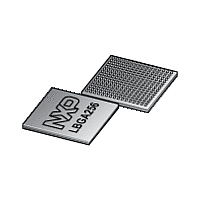
LPC1850FET256 NXP Semiconductors, LPC1850FET256 Datasheet - Page 88

LPC1850FET256
Manufacturer Part Number
LPC1850FET256
Description
The LPC1850FET256 is a high-performance, cost-effective Cortex-M3 microcontroller featuring 200 kB of SRAM, and advanced peripherals including Ethernet, High Speed USB 2
Manufacturer
NXP Semiconductors
Datasheet
1.LPC1810FBD144.pdf
(157 pages)
Available stocks
Company
Part Number
Manufacturer
Quantity
Price
Company:
Part Number:
LPC1850FET256
Manufacturer:
NXP
Quantity:
1 000
Part Number:
LPC1850FET256
Manufacturer:
NXP/恩智浦
Quantity:
20 000
Company:
Part Number:
LPC1850FET256,551
Manufacturer:
NXP Semiconductors
Quantity:
10 000
Part Number:
LPC1850FET256,551
Manufacturer:
NXP/恩智浦
Quantity:
20 000
NXP Semiconductors
LPC1850_30_20_10
Preliminary data sheet
7.18.7 System PLL1
7.18.8 Reset Generation Unit (RGU)
7.18.9 Power control
The PLL1 accepts an input clock frequency from an external oscillator in the range of
10 MHz to 25 MHz. The input frequency is multiplied up to a high frequency with a Current
Controlled Oscillator (CCO). The multiplier can be an integer value from 1 to 32. The CCO
operates in the range of 156 MHz to 320 MHz, so there is an additional divider in the loop
to keep the CCO within its frequency range while the PLL is providing the desired output
frequency. The output divider may be set to divide by 2, 4, 8, or 16 to produce the output
clock. Since the minimum output divider value is 2, it is insured that the PLL output has a
50 % duty cycle. The PLL is turned off and bypassed following a chip reset and may be
enabled by software. The program must configure and activate the PLL, wait for the PLL
to lock, and then connect to the PLL as a clock source. The PLL settling time is 100 s.
The RGU allows generation of independent reset signals for individual blocks and
peripherals.
The LPC1850/30/20/10 feature several independent power domains to control power to
the core and the peripherals (see
alarm timer, the CREG block, the OTP controller, the back-up registers, and the event
router) are located in the RTC power-domain which can be powered by a battery supply or
the main regulator. A power selector switch ensures that the RTC block is always powered
on.
All information provided in this document is subject to legal disclaimers.
Rev. 3.1 — 15 December 2011
Figure
11). The RTC and its associated peripherals (the
32-bit ARM Cortex-M3 microcontroller
LPC1850/30/20/10
© NXP B.V. 2011. All rights reserved.
88 of 157


