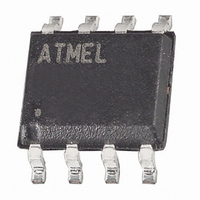
AT25DF081-SSHN-B Atmel, AT25DF081-SSHN-B Datasheet - Page 10

AT25DF081-SSHN-B
Manufacturer Part Number
AT25DF081-SSHN-B
Description
IC FLASH 8MBIT 66MHZ 8SOIC
Manufacturer
Atmel
Datasheet
1.AT25DF081-SSHN-T.pdf
(38 pages)
Specifications of AT25DF081-SSHN-B
Format - Memory
FLASH
Memory Type
DataFLASH
Memory Size
8M (4096 pages x 256 bytes)
Speed
66MHz
Interface
SPI, 3-Wire Serial
Voltage - Supply
1.65 V ~ 1.95 V
Operating Temperature
-40°C ~ 85°C
Package / Case
8-SOIC (3.9mm Width)
Cell Type
NOR
Density
8Mb
Access Time (max)
7ns
Interface Type
Serial (SPI)
Boot Type
Not Required
Address Bus
1b
Operating Supply Voltage (typ)
1.8V
Operating Temp Range
-40C to 85C
Package Type
SOIC
Sync/async
Synchronous
Operating Temperature Classification
Industrial
Operating Supply Voltage (min)
1.65V
Operating Supply Voltage (max)
1.95V
Supply Current
12mA
Mounting
Surface Mount
Pin Count
8
Architecture
Sectored
Supply Voltage (max)
1.95 V
Supply Voltage (min)
1.65 V
Maximum Operating Current
12 mA
Mounting Style
SMD/SMT
Organization
64 KB x 16
Memory Configuration
4096 Pages X 256 Bytes
Clock Frequency
66MHz
Supply Voltage Range
1.65V To 1.95V
Memory Case Style
SOIC
Rohs Compliant
Yes
Lead Free Status / RoHS Status
Lead free / RoHS Compliant
Available stocks
Company
Part Number
Manufacturer
Quantity
Price
Company:
Part Number:
AT25DF081-SSHN-B
Manufacturer:
ATMEL
Quantity:
4 300
Figure 8-1.
Figure 8-2.
8.2
10
SCK
SO
CS
Block Erase
SI
AT25DF081
Byte Program
Page Program
SCK
SO
CS
SI
MSB
HIGH-IMPEDANCE
0
0
0
1
A block of 4K-, 32K-, or 64K-bytes can be erased (all bits set to the logical “1” state) in a single
operation by using one of three different opcodes for the Block Erase command. An opcode of
20h is used for a 4K-byte erase, an opcode of 52h is used for a 32K-byte erase, and an opcode
of D8h is used for a 64K-byte erase. Before a Block Erase command can be started, the Write
Enable command must have been previously issued to the device to set the WEL bit of the Sta-
tus Register to a logical “1” state.
To perform a Block Erase, the CS pin must first be asserted and the appropriate opcode (20h,
52h, or D8h) must be clocked into the device. After the opcode has been clocked in, the three
address bytes specifying an address within the 4K-, 32K-, or 64K-byte block to be erased must
be clocked in. Any additional data clocked into the device will be ignored. When the CS pin is
deasserted, the device will erase the appropriate block. The erasing of the block is internally
self-timed and should take place in a time of t
Since the Block Erase command erases a region of bytes, the lower order address bits do not
need to be decoded by the device. Therefore, for a 4K-byte erase, address bits A11-A0 will be
ignored by the device and their values can be either a logical “1” or “0”. For a 32K-byte erase,
address bits A14-A0 will be ignored, and for a 64K-byte erase, address bits A15-A0 will be
ignored by the device. Despite the lower order address bits not being decoded by the device, the
complete three address bytes must still be clocked into the device before the CS pin is deas-
serted, and the CS pin must be deasserted on an even byte boundary (multiples of eight bits);
otherwise, the device will abort the operation and no erase operation will be performed.
0
2
OPCODE
0
HIGH-IMPEDANCE
MSB
3
0
0
0
4
0
1
0
5
0
2
OPCODE
1
6
0
3
0
7
0
MSB
4
A
ADDRESS BITS A23-A0
8
0
5
A
9
1
6
A
0
7
MSB
A
8
A
A
29 30
9
ADDRESS BITS A23-A0
A
A
10 11
A
A
31 32
MSB
A
D
12
A
D
33
DATA IN BYTE 1
D
34
D
35
A
29 30
D
BLKE
36
A
D
37 38
A
.
31 32
D
MSB
D
D
39
D
33
D
34
DATA IN
D
35
MSB
D
D
36
D
DATA IN BYTE n
D
37 38
D
D
D
D
39
D
D
D
D
3674E–DFLASH–8/08


