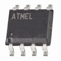
AT25DF081-SSHN-B Atmel, AT25DF081-SSHN-B Datasheet - Page 17

AT25DF081-SSHN-B
Manufacturer Part Number
AT25DF081-SSHN-B
Description
IC FLASH 8MBIT 66MHZ 8SOIC
Manufacturer
Atmel
Datasheet
1.AT25DF081-SSHN-T.pdf
(38 pages)
Specifications of AT25DF081-SSHN-B
Format - Memory
FLASH
Memory Type
DataFLASH
Memory Size
8M (4096 pages x 256 bytes)
Speed
66MHz
Interface
SPI, 3-Wire Serial
Voltage - Supply
1.65 V ~ 1.95 V
Operating Temperature
-40°C ~ 85°C
Package / Case
8-SOIC (3.9mm Width)
Cell Type
NOR
Density
8Mb
Access Time (max)
7ns
Interface Type
Serial (SPI)
Boot Type
Not Required
Address Bus
1b
Operating Supply Voltage (typ)
1.8V
Operating Temp Range
-40C to 85C
Package Type
SOIC
Sync/async
Synchronous
Operating Temperature Classification
Industrial
Operating Supply Voltage (min)
1.65V
Operating Supply Voltage (max)
1.95V
Supply Current
12mA
Mounting
Surface Mount
Pin Count
8
Architecture
Sectored
Supply Voltage (max)
1.95 V
Supply Voltage (min)
1.65 V
Maximum Operating Current
12 mA
Mounting Style
SMD/SMT
Organization
64 KB x 16
Memory Configuration
4096 Pages X 256 Bytes
Clock Frequency
66MHz
Supply Voltage Range
1.65V To 1.95V
Memory Case Style
SOIC
Rohs Compliant
Yes
Lead Free Status / RoHS Status
Lead free / RoHS Compliant
Available stocks
Company
Part Number
Manufacturer
Quantity
Price
Company:
Part Number:
AT25DF081-SSHN-B
Manufacturer:
ATMEL
Quantity:
4 300
9.6
3674E–DFLASH–8/08
Read Sector Protection Registers
If the desire is to only change the SPRL bit without performing a Global Protect or Global Unpro-
tect, then the system can simply write a 0Fh to the Status Register to change the SPRL bit from
a logical “1” to a logical “0” provided the WP pin is deasserted. Likewise, the system can write an
F0h to change the SPRL bit from a logical “0” to a logical “1” without affecting the current sector
protection status (no changes will be made to the Sector Protection Registers).
When writing to the Status Register, bits 5, 4, 3, and 2 will not actually be modified but will be
decoded by the device for the purposes of the Global Protect and Global Unprotect functions.
Only bit 7, the SPRL bit, will actually be modified. Therefore, when reading the Status Register,
bits 5, 4, 3, and 2 will not reflect the values written to them but will instead indicate the status of
the WP pin and the sector protection status. Please refer to the “Read Status Register” section
and
read for bits 5, 4, 3, and 2.
The Sector Protection Registers can be read to determine the current software protection status
of each sector. Reading the Sector Protection Registers, however, will not determine the status
of the WP pin.
To read the Sector Protection Register for a particular sector, the CS pin must first be asserted
and the opcode of 3Ch must be clocked in. Once the opcode has been clocked in, three address
bytes designating any address within the sector must be clocked in. After the last address byte
has been clocked in, the device will begin outputting data on the SO pin during every subse-
quent clock cycle. The data being output will be a repeating byte of either FFh or 00h to denote
the value of the appropriate Sector Protection Register
Table 9-3.
Deasserting the CS pin will terminate the read operation and put the SO pin into a high-imped-
ance state. The CS pin can be deasserted at any time and does not require that a full byte of
data be read.
In addition to reading the individual Sector Protection Registers, the Software Protection Status
(SWP) bit in the Status Register can be read to determine if all, some, or none of the sectors are
software protected (please refer to
Output Data
Table 10-1 on page 20
FFh
00h
Read Sector Protection Register – Output Data
Sector Protection Register Value
Sector Protection Register value is 0 (sector is unprotected).
Sector Protection Register value is 1 (sector is protected).
for details on the Status Register format and what values can be
“Status Register Commands” on page 20
AT25DF081
for more details).
17


