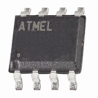
AT25DF081-SSHN-B Atmel, AT25DF081-SSHN-B Datasheet - Page 4

AT25DF081-SSHN-B
Manufacturer Part Number
AT25DF081-SSHN-B
Description
IC FLASH 8MBIT 66MHZ 8SOIC
Manufacturer
Atmel
Datasheet
1.AT25DF081-SSHN-T.pdf
(38 pages)
Specifications of AT25DF081-SSHN-B
Format - Memory
FLASH
Memory Type
DataFLASH
Memory Size
8M (4096 pages x 256 bytes)
Speed
66MHz
Interface
SPI, 3-Wire Serial
Voltage - Supply
1.65 V ~ 1.95 V
Operating Temperature
-40°C ~ 85°C
Package / Case
8-SOIC (3.9mm Width)
Cell Type
NOR
Density
8Mb
Access Time (max)
7ns
Interface Type
Serial (SPI)
Boot Type
Not Required
Address Bus
1b
Operating Supply Voltage (typ)
1.8V
Operating Temp Range
-40C to 85C
Package Type
SOIC
Sync/async
Synchronous
Operating Temperature Classification
Industrial
Operating Supply Voltage (min)
1.65V
Operating Supply Voltage (max)
1.95V
Supply Current
12mA
Mounting
Surface Mount
Pin Count
8
Architecture
Sectored
Supply Voltage (max)
1.95 V
Supply Voltage (min)
1.65 V
Maximum Operating Current
12 mA
Mounting Style
SMD/SMT
Organization
64 KB x 16
Memory Configuration
4096 Pages X 256 Bytes
Clock Frequency
66MHz
Supply Voltage Range
1.65V To 1.95V
Memory Case Style
SOIC
Rohs Compliant
Yes
Lead Free Status / RoHS Status
Lead free / RoHS Compliant
Available stocks
Company
Part Number
Manufacturer
Quantity
Price
Company:
Part Number:
AT25DF081-SSHN-B
Manufacturer:
ATMEL
Quantity:
4 300
3. Block Diagram
4. Memory Array
4
Figure 2-1.
GND
WP
SO
CS
AT25DF081
HOLD
1
2
3
4
SCK
8-SOIC Top View
WP
SO
CS
SI
8
7
6
5
To provide the greatest flexibility, the memory array of the AT25DF081 can be erased in four lev-
els of granularity including a full chip erase. In addition, the array has been divided into physical
sectors of uniform size, of which each sector can be individually protected from program and
erase operations. The size of the physical sectors is optimized for both code and data storage
applications, allowing both code and data segments to reside in their own isolated
regions.
down of each physical sector.
VCC
HOLD
SCK
SI
INTERFACE
CONTROL
LOGIC
AND
Figure 4-1 on page 5
Figure 2-2.
GND
WP
SO
CS
PROTECTION LOGIC
1
2
3
4
CONTROL AND
8-UDFN Top View
illustrates the breakdown of each erase level as well as the break-
X-DECODER
Y-DECODER
8
7
6
5
VCC
HOLD
SCK
SI
Figure 2-3.
AND LATCHES
I/O BUFFERS
MEMORY
ARRAY
Y-GATING
FLASH
C
D
A
B
E
F
DATA BUFFER
11-dBGA (Top View
Through Back of Die)
NC
1
HOLD
SRAM
VCC
SCK
SI
2
GND
WP
CS
SO
3
NC
NC
3674E–DFLASH–8/08
4


