APMOTOR56F8000E Freescale Semiconductor, APMOTOR56F8000E Datasheet - Page 19
APMOTOR56F8000E
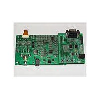
Manufacturer Part Number
APMOTOR56F8000E
Description
KIT DEMO MOTOR CTRL SYSTEM
Manufacturer
Freescale Semiconductor
Type
Motor / Motion Controllers & Driversr
Datasheets
1.CWH-UTP-ONCE-HE.pdf
(2 pages)
2.APMOTOR56F8000E.pdf
(124 pages)
3.APMOTOR56F8000E.pdf
(2 pages)
Specifications of APMOTOR56F8000E
Accessory Type
Motor Controller
Input Voltage
9 V
Interface Type
RS-232
Product
Power Management Modules
For Use With/related Products
DEMO56F8013, DEMO56F8013-E
Lead Free Status / RoHS Status
Lead free / RoHS Compliant


Freescale Semiconductor
Table 2-3 56F8014 Signal and Package Information for the 32-Pin LQFP (Continued)
2. This signal is also brought out on the GPIOB0 pin.
Return to
(GPIOA7)
GPIOB7
GPIOB4
(CLKO)
RESET
Signal
(SCL
Name
(TXD)
(T0)
2
)
Table 2-2
Pin No.
LQFP
16
19
2
Input/Open
Output
Output
Output
Output
Output
Output
Output
Input/
Input/
Input/
Input/
Input/
Type
Drain
Input
State During
Input with
Input with
Input with
enabled
enabled
enabled
internal
internal
internal
pull-up
pull-up
pull-up
Reset
56F8014 Technical Data, Rev. 11
Port B GPIO — This GPIO pin can be individually programmed as
an input or output pin.
Transmit Data — SCI transmit data output or transmit / receive in
single wire opeation.
Serial Clock — This pin serves as the I
After reset, the default state is GPIOB7. The alternative peripheral
functionality is controlled via the SIM. See
Reset — This input is a direct hardware reset on the processor.
When RESET is asserted low, the chip is initialized and placed in the
reset state. A Schmitt trigger input is used for noise immunity. The
internal reset signal will be deasserted synchronous with the internal
clocks after a fixed number of internal clocks.
Port A GPIO — This GPIO pin can be individually programmed as
an input or open drain output pin. Note that RESET functionality is
disabled in this mode and the chip can only be reset via POR, COP
reset, or software reset.
After reset, the default state is RESET.
Port B GPIO — This GPIO pin can be individually programmed as
an input or output pin.
T0 — Timer, Channel 0
Clock Output — This is a buffered clock signal. Using the
SIM_CLKO Select Register (SIM_CLKOSR), this pin can be
programmed as any of the following: disabled (logic 0), CLK_MSTR
(system clock), IPBus clock, or oscillator output. See
After reset, the default state is GPIOB4. The alternative peripheral
functionality is controlled via the SIM. See
Signal Description
2
C serial clock.
Section
Section
6.3.8.
6.3.8.
Section
56F8014 Signal Pins
6.3.7.
19
Related parts for APMOTOR56F8000E
Image
Part Number
Description
Manufacturer
Datasheet
Request
R

Part Number:
Description:
Manufacturer:
Freescale Semiconductor, Inc
Datasheet:
Part Number:
Description:
Manufacturer:
Freescale Semiconductor, Inc
Datasheet:
Part Number:
Description:
Manufacturer:
Freescale Semiconductor, Inc
Datasheet:
Part Number:
Description:
Manufacturer:
Freescale Semiconductor, Inc
Datasheet:
Part Number:
Description:
Manufacturer:
Freescale Semiconductor, Inc
Datasheet:
Part Number:
Description:
Manufacturer:
Freescale Semiconductor, Inc
Datasheet:
Part Number:
Description:
Manufacturer:
Freescale Semiconductor, Inc
Datasheet:
Part Number:
Description:
Manufacturer:
Freescale Semiconductor, Inc
Datasheet:
Part Number:
Description:
Manufacturer:
Freescale Semiconductor, Inc
Datasheet:
Part Number:
Description:
Manufacturer:
Freescale Semiconductor, Inc
Datasheet:
Part Number:
Description:
Manufacturer:
Freescale Semiconductor, Inc
Datasheet:
Part Number:
Description:
Manufacturer:
Freescale Semiconductor, Inc
Datasheet:
Part Number:
Description:
Manufacturer:
Freescale Semiconductor, Inc
Datasheet:
Part Number:
Description:
Manufacturer:
Freescale Semiconductor, Inc
Datasheet:
Part Number:
Description:
Manufacturer:
Freescale Semiconductor, Inc
Datasheet: